|
IA-64 Workstation SDV Beta User’s Guide |
Revision:
1.1 – Jan 0
Contents
1 WARNINGS
*Warning Summary
*2 Introduction
*Chassis Description
*Chassis Features Summary
*Chassis Front Controls and Indicators
*Chassis Rear Controls and Features
*Peripheral Bay
*LS-120 Drive
*CD-ROM Drive
*Hard Drive Bay
*Power Supply
*System Cooling
*Start-Up -- Video Monitor / System
*Upgrading PCI Cards and Memory
*Accessing the PCI Slots and Memory Boards
*Adding PCI cards
*Removing the Memory Board
*Adding Memory
*Removing Memory
*Valid Memory Configurations
*3 Board Set Description
*Board Set Features
*Processor Overview
*Memory Overview
*DIMM Installation Sequence
*Peripherals
*Super I/O Chip
*Baseboard Connectors
*PCI
*AGP
*Video
*SCSI Controller
*IDE Controller
*Keyboard and Mouse
*Front Panel
*4 BIOS - Overview
*BIOS Flash Memory Organization
*Resource Configuration
*Plug and Play: PCI Auto-configuration
*PCI IDE Support
*System Management BIOS (SMBIOS)
*BIOS Upgrades
*Preparing for the Upgrade
*Obtaining the BIOS Upgrade File
*Creating the BIOS Upgrade Diskette
*Upgrading the System BIOS
*Recovering the BIOS
*Language Support
*Boot Options
*Post Codes
*POST Codes Testing Phase
*5 Solving Problems
*Resetting the System
*Initial System Startup
*Startup Checklist
*Monitoring POST
*Verifying Proper Operation of Key System Lights
*Network Problems
*PCI Installation Tips
*Error and Informational Messages
*Specific Problems and Corrective Actions
*Power Light Does Not Light
*System Boots Very Slowly
*No Characters Appear on the Screen
*Characters Are Distorted or Incorrect
*System Cooling Fans Do Not Rotate Properly
*LS-120 Drive Activity Light Does Not Light
*Hard Disk Drive Activity Light Does Not Light
*CD-ROM Drive Activity Light Does Not Light
*Speaker
*BIOS Beep Codes
*Network Problems
*PCI Installation Tips
*Bootable CD-ROM Is Not Detected
*Error and Informational Messages
*6 Technical Reference
*Processor Board Connectors
*Baseboard Connectors
*AGP Pro Connector
*Other Baseboard Connectors
*Baseboard Power Input Connectors
*Memory Board Connectors
*7 I/O Board Connectors
*Keyboard and Mouse Connectors
*Serial Port Connector
*Front Panel Connector
*IDE Connectors
*Hard Drive LED Header
*Speaker Connector
*Chassis Intrusion Header
*USB Port
*USB Header
*Rear I/O Audio Line-in Connector
*Rear I/O Audio Line-out Connector
*CD in Header
*Front Panel Mic in
*Front Panel Line-in
*8 Jumper Settings
*Clocks
*
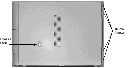
Figure 1. Workstation System Chassis
*Figure 2. Front Controls and Indicators
*Figure 3. Chassis Rear View
*Figure 4. Processor E-PAC
*Figure 5. E-PAC Cooling Zones
*Figure 6. EFI Shell Prompt
*Figure 7. Chassis Side Cover
*Figure 8. Power Supply door
*Figure 9
. PCI Slots and Memory Boards *Figure 10. Adding Memory
*Figure 11.
Memory Board Stacks *Figure 12. Board Set Overview
*Figure 13. Memory Expansion Card
*Figure 14. Baseboard Connectors
*Figure 15. Baseboard Connectors
*Figure 16. Keyboard and Mouse Connectors
*Figure 17. Serial Port Connector Pin out
*Figure 18. Boot Jumper
*
Table 1. Physical Specifications
*Table 2. Chassis Features Summary
*Table 3. Front Panel Components
*Table 4. Chassis Rear Components
*Table 5. Board Set Features
*Table 6. Tested Memory
*Table 7. Workstation Board BIOS Features
*Table 8. POST Codes
*Table 9. ITP Connector
*Table 10. Processor Board Connector
*Table 11. I/O Board Connector
*Table 12. AGP Pro Connector
*Table 13. Fan connectors
*Table 14. Thermistor Connector
*Table 15. Baseboard to Processor Board Connector
*Table 16. Baseboard to Memory Board Connectors
*Table 17. PCI Connectors
*Table 18. 24-Pin Power Connector
*Table 19. 22-Pin Power Connector
*Table 20. 8-Pin Power Connector
*Table 21. DIMM Connector
*Table 22. DC-DC Converter Connector
*Table 23. Keyboard and Mouse Connector Pin outs
*Table 24. Serial Port Connector Pin out
*Table 25. Front Panel Connector
*Table 26. IDE Connector
*Table 27. Hard drive LED Header
*Table 28. Speaker Connector
*Table 29. Chassis Intrusion Header
*Table 30. USB Port
*Table 31. USB Header
*Table 32. Rear I/O Audio Line-in Connector
*Table 33. Rear I/O Audio Line-out Connector
*Table 34. CD In Header
*Table 35. Front Panel Mic in
*Table 36. Front Panel Line-in
*Table 37
. CACHE Enable (J6C1-IO Card) *Table 38. Clock Jumper Selection
*Table 39. JTAG Header (
J9E1 - FSB Connector) *Table 40. Boot Jumper Header (J1G2 )
*Table 41. JTAG MEMA (J5-G1-MEMA)
*Table 42. JTAG MEMB (J7-D1-MEMB)
*
Acronyms
|
Acronyms |
Meaning |
Acronyms |
Meaning |
Acronyms |
Meaning |
Acronyms |
Meaning |
|
ACPI |
Advanced Configuration and Power Interface |
ECC |
Error Checking and Correcting |
IRQ |
Interrupt Request |
POST |
Power-On Self Test |
|
ADPCM |
Adaptive Differential Pulse Code Modulation |
ECHS |
Extended Cylinder Head Sector |
LAN |
Local Area Network |
SCI |
Special Circumstance Instructions |
|
AGP |
Accelerated Graphics Port |
ECP |
Extended Capabilities Port |
LBA |
Logical Block Addressing |
SIR |
Surface Insulation Resistance |
|
APM |
Advanced Power Management |
EMC |
Electro-Magnetic Compatibility |
LED |
Light Emitting Diode |
SMI |
System Management Interrupt |
|
BIOS |
Basic Input / Output System |
ESCD |
Extended System Configuration Data |
MHz |
MegaHertz |
SMM |
System Management Mode |
|
CMOS |
Complementary Metal Oxide Semiconductor |
ESD |
Electrostatic Discharge |
MIF |
Management Information Format |
SMP |
Symmetric Multi-Processing |
|
CPU |
Central Processing Unit. (Now at IntelÒ referred to as a processor.) |
FIFO |
First In, First Out |
MIDI |
Musical Instrument Digital Interface |
SRAM |
Static Random Access Memory |
|
CSMA/CD |
Carrier Sense Multiple Access with Collision Detection |
IDE |
Integrated Dual Channel Enhanced |
MTBF |
Mean Time Between Failures |
UHCI |
Universal Host Controller Interface |
|
DIMM |
Dual Inline Memory Module |
I/O |
Input / Output |
NIC |
Network Interface Card |
USB |
Universal Serial Bus |
|
DMA |
Direct Memory Access |
IOAPIC |
Input / Output Advanced Programmable Input Controller |
OEM |
Original Equipment Manufacturer |
VID |
Voltage ID |
|
DMI |
Desktop Management Interface |
IPL |
Initial Program Load |
OS |
Operating System |
VPD |
Vital Product Data |
|
DRAM |
Dynamic Random Access Memory |
PAC |
P CI A.G.P. Controller |
WfM |
Wired for Management |
||
|
PCI |
Peripheral Component Interconnect |
|
|
The power supply in this product contains no user-serviceable parts. Refer servicing only to qualified personnel. |
|
|
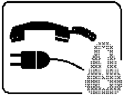
Do not attempt to modify or use the supplied AC power cord if it is not the exact type required. |
|
|
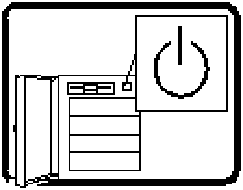
The DC push-button on/off switch on the system does not turn off system AC power. To remove AC power from the system, you must unplug each AC power cord from the wall outlet or power supply. |
|
|
SAFETY STEPS - Whenever you remove the chassis covers to access the inside of the system, follow these steps:
|
|
|
After you have completed the six SAFETY steps above, you can remove the system covers. To do this:
|
|
|
For proper cooling and airflow, always reinstall the chassis covers before turning on the system. Operating the system without the covers in place can damage system parts. To install the covers:
|
|
|
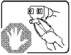
The microprocessor, heat sink and power pod may be hot if the system has been running. Also, there may be sharp pins and edges on some board and chassis parts. Contact should be made with care. Consider wearing protective gloves. |
|
|
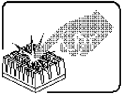
Danger of explosion if the battery is incorrectly replaced. Replace only with the same or equivalent type recommended by the equipment manufacturer. Discard used batteries according to manufacturer’s instructions.
|
|
|
The system is designed to operate in a typical office environment. Choose a site that is:
|
(This Page Left Intentionally Blank)
The Workstation SDV Beta version, has been developed as a platform that can be used for developing operating systems, software and device drivers for Itanium™ processor-based systems and the IA-64 Instruction Set Architecture (ISA). The Workstation SDV features the Intel® 82460GX PCI set, multiple 33 MHz PCI expansion slots and large memory capacity. Future revisions of the Workstation SDV will support AGP Pro* 110 graphics cards and 64-bit/66 MHz PCI.
The Workstation SDV is configured as follows:
/
NOTESystem upgrades will be made throughout the SDV program.
The beta Workstation SDV is housed in a WTX compliant chassis. It is designed to accommodate the needs of a variety of high-performance applications. As application requirements increase, the system can be upgraded with:
Table 1. Physical Specifications
|
Specification |
Value |
|
Height |
44.45 cm (17.5 inches) without feet 45.72 cm (18 inches) with standard feet |
|
Width |
25.40 cm (10 inches) |
|
Depth |
64.52 cm (25.4 inches) |
|
Weight |
38.18 kg (84 lbs.) |
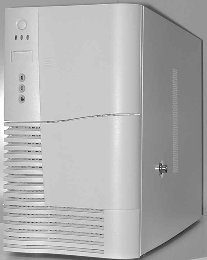
Figure 1. Workstation System Chassis
Table 2. Chassis Features Summary
|
Feature |
Comment |
|
Power system |
An 800-watt power supply that is capable of operating over input voltage ranges of 100-240 VAC. Includes two- (2) integrated 80mm fans for cooling. |
|
Workstation chassis |
Designed to operate in a standard office environment. Mid-tower (desk side) design capable of operating from a standard AC power outlet. |
|
Peripheral bay can accommodate up to three- (3), 5.25-inch media and one- (1), 3.5-inch media devices. |
|
|
The hard drive bay accepts 3.5-inch-wide drives. It can accommodate up to five- (5), 1-inch or three- (3), 1.6-inch devices. |
|
|
The plastic front bezel provides airflow and easy access to the peripheral and hard drive bays. The removable top & side covers provide proper airflow and easy access to components inside the system. Only technically qualified personnel should remove the system covers. |
|
|
Cooling system |
The system has provisions for up to nine- (9) fans for cooling within three- (3) separate cooling zones. There are two- (2), 120mm fans, three- (3), 80mm fans and three- (3), 60mm fans. One additional 80mm fan is used for cooling the two memory boards. |
|
System security |
A side lock and chassis intrusion switch provides security against system tampering. The intrusion switch can be used with system level software (when it becomes available) to warn of chassis intrusion. |
Chassis Front Controls and Indicators
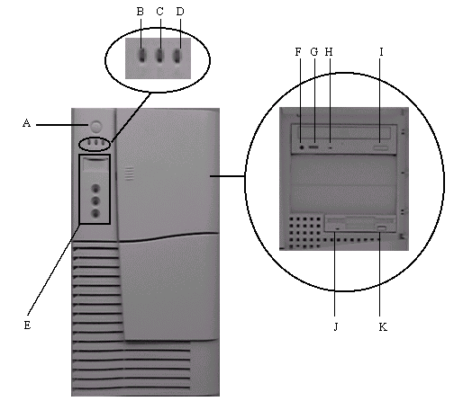
Figure 2. Front Controls and Indicators
Table 3. Front Panel Components
|
Item |
Feature/Description |
|
Front Panel |
|
|
A. |
Power Switch |
|
B. |
Power LED |
|
C. |
Drive activity LED |
|
D. |
LAN LED (Not used at present time) |
|
E. |
Not used |
|
CD-ROM Drive |
|
|
F. |
Headphone Jack |
|
G. |
Volume control |
|
H. |
Activity LED |
|
I. |
Open/Close button |
|
3.5-inch Diskette Drive (LS-120) |
|
|
J. |
Activity LED |
|
K. |
Ejector button |
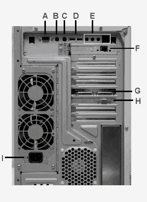
Chassis Rear Controls and Features
|
Item |
Feature/Description |
|
A. |
Serial port |
|
B. |
PS/2-compatible, 6-pin keyboard connector |
|
C. |
PS/2 compatible, 6-pin mouse connector |
|
D. |
Two- (2) USB ports, 4-pin connector - validated |
|
E. |
Not Used |
|
F. |
PCI LAN card (Intel* D101M Ethernet) |
|
G. |
One- (1) SCSI Qlogic* 1280 card |
|
H. |
PCI video card (ATI Rage 128GL) |
|
I |
Reset Switch |
Note:
Peripheral Bay
The peripheral bay can accommodate one- (1), 3.5-inch and three- (3), 5.25-inch devices. The CD-ROM and the LS-120 drives are housed in the peripheral bay. Both devices are accessible from the front of the chassis (Refer to Figure 2).
The LS-120 drive (located in the peripheral bay), supports 120MB and 1.44 MB media. For the Workstation SDV the device used is the Mitsubishi* MF357G-31111UAL (IDE).
In the Workstation SDV system, the CD-ROM drive in the peripheral bay consists of an IDE device in the form of a TEAC CD-532EB running at 32X.
The hard drive bay is designed for 3.5-inch-wide hard drives. It can accommodate up to five- (5), 1-inch-high or three- (3), 1.6-inch-high drives. The Workstation SDV system includes one- (1) Quantum* KN09L011-01-A-E SCSI hard drive. The drive has a storage capacity of 9.1 GB.
The chassis is configured with a single, 800-watt power supply. It is capable of providing full rated output power over a range of input voltages: 100-240 VAC. The power supply features automatic Power Factor Correction (PFC), and is connected to the system boards using the following connectors:
For ease of replacement, the connectors can be disconnected from the supply and the supply replaced without the need for removing the system boards or unhooking any connectors from the boards.
System Cooling
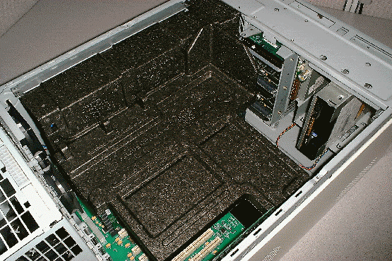
The Workstation SDV system has three- (3) cooling zones: processor, memory and I/O zones.
In addition, the power supply also has two- (2), internal 80mm fans for cooling.
Processor E-PAC
Baseboard E-PAC
/
NOTEAll chassis covers must be on the system for proper cooling. The black foam material that is found inside the chassis is an integral part of the cooling system. The system must not be operated without this material in place. System damage may occur.
Start-Up -- Video Monitor / System
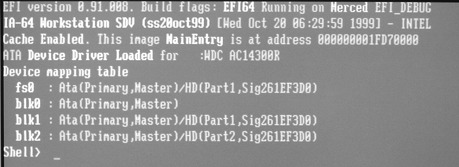
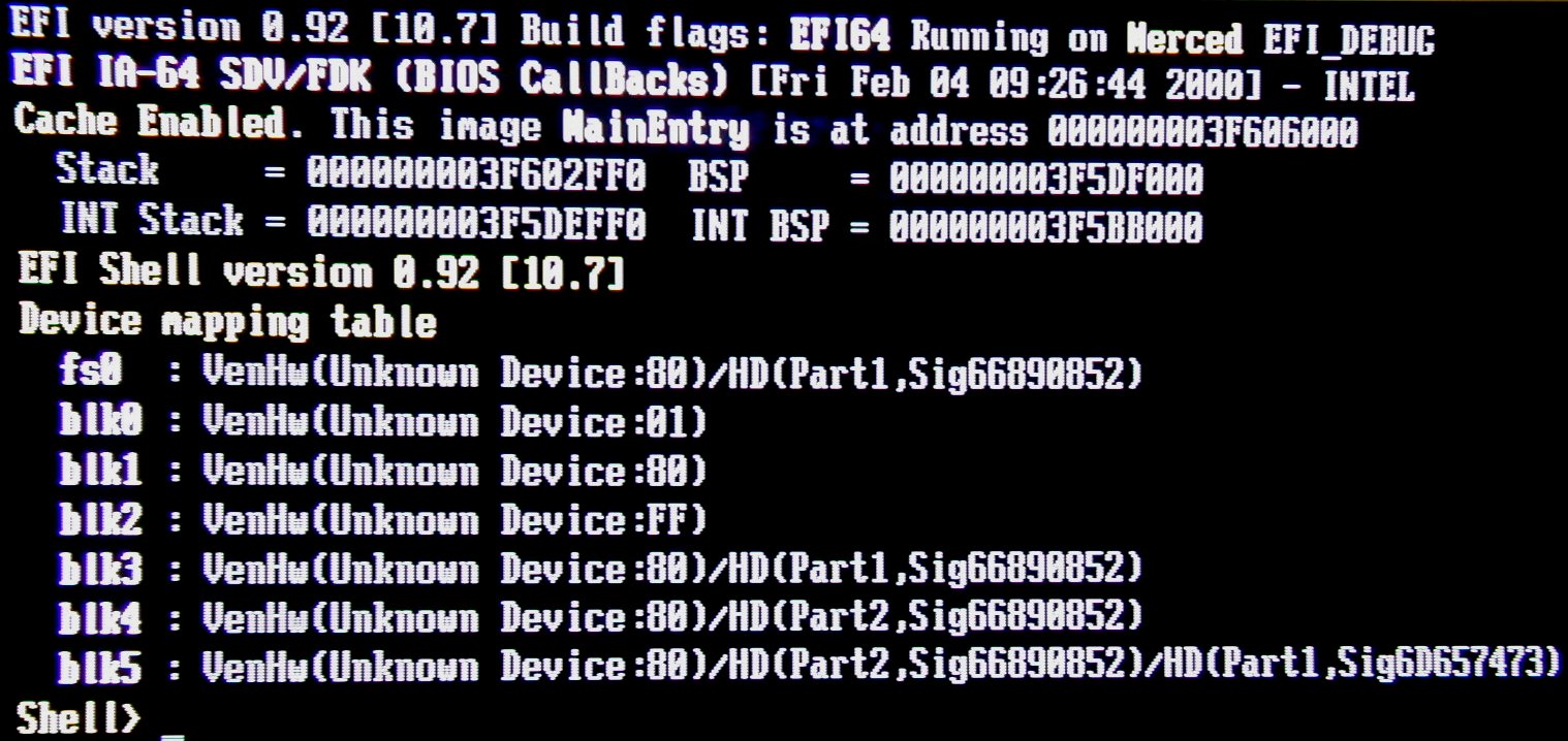
Figure 6. EFI Shell Prompt
/
NOTEAnNo operating system is not pre-loaded on the system.
Upgrading PCI Cards and Memory
In order to add or remove PCI cards and memory, the side cover of the system must be removed and the power supply door opened to allow access to the required components on the baseboard.
![]() CAUTION
CAUTION
Before removing or installing the Workstation SDV board or any other system component, observe all the safety guidelines for safety requirements and precautions. Always follow the steps in the procedure in the correct order (i.e., as written). Set up a log to record identification information about your computer. When working on any Workstation SDV board, wear an anti-static wrist wrap and place the board on a conductive foam pad.
![]() WARNINGS
WARNINGS
The procedures in this section assume that you are familiar with the general terminology associated with personal computers and with the safety practices and regulatory compliance required for using and modifying electronic equipment including, but not limited to the following:
![]() CAUTION
CAUTION
Electrostatic discharge (ESD) can damage components. Therefore, protect
against ESD by performing the procedures described in this section only at an ESD workstation or by wearing an anti-static wrist wrap and attaching it to a metal part of your computer’s chassis.
Accessing the PCI Slots and Memory Boards
The system must be powered down and the power cord must be disconnected before attempting to remove the side cover. In addition, please adhere to all safety and regulatory procedures. To gain access to the PCI slots and memory boards refer to Figure 7 and Figure 8.
Figure 7. Chassis Side Cover

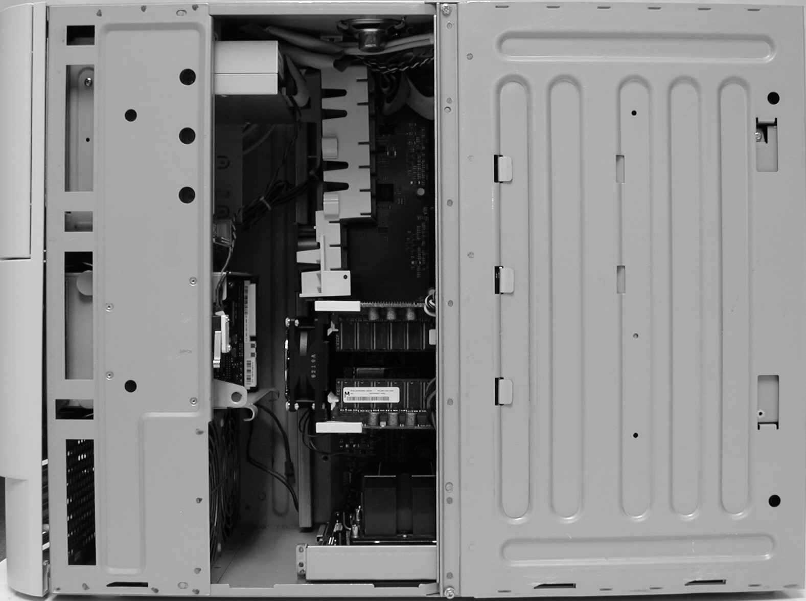
Figure 8. Power Supply door
The Workstation SDV has seven- (7) PCI slots as shown in Figure 9. To install a PCI add-in card, identify an empty PCI slot and insert the card into the slot. When the card is properly seated, press the card into the slot until it is firmly in place.
To add or remove memory, each memory board must be removed from the baseboard connector. Remove a memory board by first pulling back the two- (2) ejector clips on the board (Refer to Figure 9). Then slide the board out of the connector and the retention mechanism.
To reinsert the memory board, align it with the guides in the retention mechanism and slide it forward. Once the board is aligned with the connector on the baseboard, press down on the ejector clips until firmly in place.
The Workstation SDV uses PC100 compliant 168-pin (x72) DIMMs. Functionally, 16-Mb, 64-Mb, 128-Mb and 256-Mb SDRAM devices are supported, but the 16-and 64-MB devices will not be validated on the system. The following steps take you through the DIMMs installation procedure (Refer to Figure 10):
Figure 10. Adding Memory
The procedure for removing memory follows:
The system can operate with one- (1) to two- (2) memory boards installed. However, to gain maximum memory bandwidth, both boards must be used. Each board has eight- (8) DIMM sites. The top four- (4) DIMMs form the top or right stack while the bottom four- (4) DIMMs form the bottom or left stack (on each of the two boards). The chipset allows multiple rows per stack, but on this system there is only one- (1) row per stack. The DIMMs within a row must be of the same size, type and must be manufactured by the same vendor. The DIMMs must always be installed in groups of four- (4).
If a single memory board is used, a minimum of four- (4) DIMMs must be populated in the top stack. If eight- (8) DIMMs are used, they can be on the same memory board in the top and bottom stacks. However, to get the maximum bandwidth with eight- (8) DIMMs, both boards should be used. The top stacks on each of the two- (2) memory boards should be populated using four- (4) DIMMs.
.
NOTEThe bottom stack in the Workstation SDV has not been activated at this time.
(This Page Left Intentionally Blank)
The architecture of the Workstation SDV supports Symmetrical Multiprocessing (SMP). However, the SDV system supports only single processor configurations. The system comes with Peripheral Component Interconnect (PCI) buses, with the board set consisting of a set of printed circuit boards:
|
A. |
I/O Board |
|
B. |
Baseboard |
|
C. |
Memory Expansion Cards |
|
D. |
Processor Board |
|
Feature |
Description |
|
|
Baseboard |
The baseboard provides the interface for the processor board, memory expansion cards, I/O board, PCI peripherals and AGP Pro. |
|
|
Processor board |
The processor board can support a maximum of two- (2), Itanium™ processors and an ITP connector. An add-in bus terminator is not required for single processor configurations. |
|
|
Itanium™ processor |
Up to two- (2) Itanium™ processors. Only one- (1) Itanium™ processor is supported on the Workstation SDV system. |
|
|
Power Pod |
Can support up to two- (2) Power Pods to supply power to the Itanium™ processors, As this system is supplied with only one- (1) Itanium™ processor, the processor board is populated with one- (1) power pod. |
|
|
Memory Expansion Cards |
Two- (2) plug-in expansion cards supporting PC100 registered SDRAM containing interleaved pathways to main memory. Each memory card supports from 256 MB to 8 GB of error correction code (ECC) memory using eight- (8), 72-bit dual inline memory modules (DIMMs). These modules interface to the baseboard through 300-pin connectors. |
|
|
I/O Board |
The I/O Board plugs into the SC242 connector at the left side of the baseboard (PCI connectors oriented top). |
|
|
The PCI-enhanced Integrated Drive Electronics (IDE) interface supports one- (1) primary and one- (1) secondary IDE channel. |
||
|
PS/2-compatible keyboard/mouse controller. |
||
|
Four- (4) universal serial bus (USB) ports. Two- (2) rear I/O USB connectors and a header for two- (2) front panel USB ports (front panel USB not supported at this time on Workstation SDV systems). |
||
|
PS/2-compatible keyboard and mouse ports (interchangeable). |
||
|
One- (1) PS/2-compatible, 9-pin serial port |
||
|
Front panel |
The front panel provides the user interface to the system |
|
|
Push-button switch controls power |
||
|
LEDs indicate power and hard drive activity |
||
Processor Overview
The Itanium™ processor is the first in a series of high-performance Intel 64-bit processors. Intel’s 64-bit Instruction Set Architecture (ISA) is referred to as IA-64. IA-64 maintains full compatibility with Intel’s current 32-bit Intel Architecture processor family while delivering industry-leading performance beyond existing architectures.
Each Itanium™ processor is packaged in a PAC418 (418-pin array cartridge) format. The cartridge includes:
/
NOTEEach processor implements the MMX™ and SSE (Streaming SIMD Extensions) technology.
Memory Overview
Main memory resides on two- (2) add-in boards called Memory Expansion Cards (MECs). Each MEC contains slots for eight- (8) DIMMs and two- (2) connectors for DC-DC converters and is attached to the baseboard through a 300-pin connector. The memory controller supports PC100-registered SDRAM DIMMs. The Workstation SDV is provided with eight- (8), 128-MB DIMMs for a total of 1 GB of memory.
/
NOTEDIMMs must be installed in groups of four- (4) with all DIMMs within a row being of the same size, type and manufacturer. For optimum performance, the rows must also be populated in the proper order with the same size of DIMMs. Depending on how the memory modules are installed, the memory subsystem can operate in two- (2) different modes; interleaved and single-port.
A single MEC supports a DIMM population in various configurations (empty sockets included). However, the DIMMs must be installed within groups of four- (4). For optimum performance, both memory cards should be installed with the top four- (4) DIMM slots populated with the same size, type and brand of memory. This recommendation utilizes both memory ports and achieves maximum memory bandwidth. The minimum memory configuration is illustrated in Figure 13.
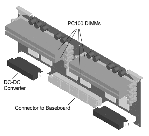
Figure 13. Memory Expansion Card
/
NOTEMaximum capacity is limited to 16 GB with two- (2) memory cards installed (using 1 GB DIMMs). However, this configuration has not been validated.
/
NOTEDIMM sizes and compatibility:
Use DIMMs that have been tested for compatibility. (Refer to Table 6.)|
Table 6. Tested Memory |
|
|
Manufacturer |
Part Number |
|
NEC Electronics, Inc. |
NC4516CC726-A80 |
|
NEC Electronics, Inc. |
MC4516-CD646-A80 |
|
Samsung Corning, Co., Ltd. |
KMM374S1623CT-GH |
/
NOTEDo not mix memory types, sizes or vendors when upgrading memory. Populate all DIMM sites with identical components.
The LPC47B27 Super I/O device supports one- (1) serial port and PS/2-compatible keyboard and mouse components. The system provides the connector interface for each port. Neither parallel ports nor FDD is supported.
The system features a single serial port located on the rear I/O panel.
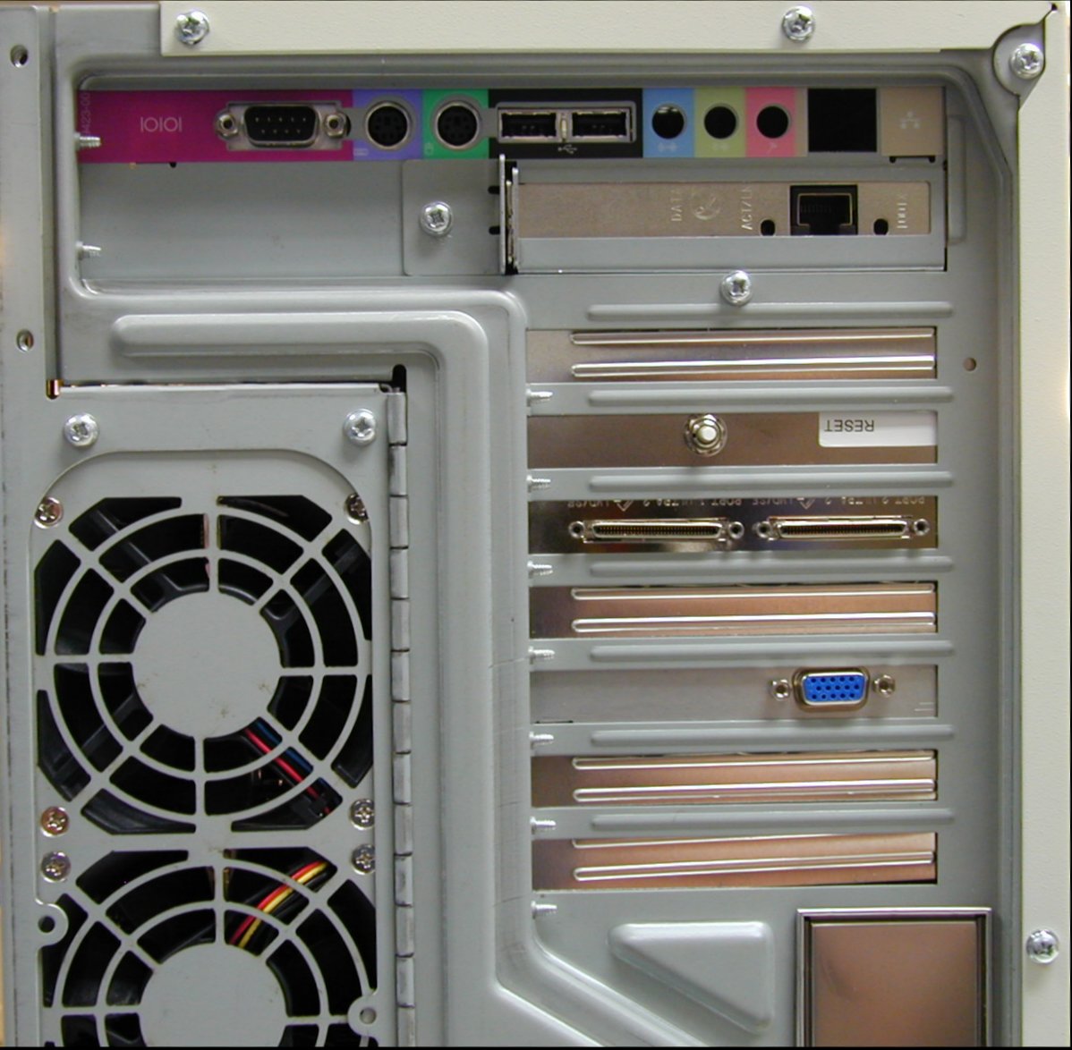
Baseboard Connectors
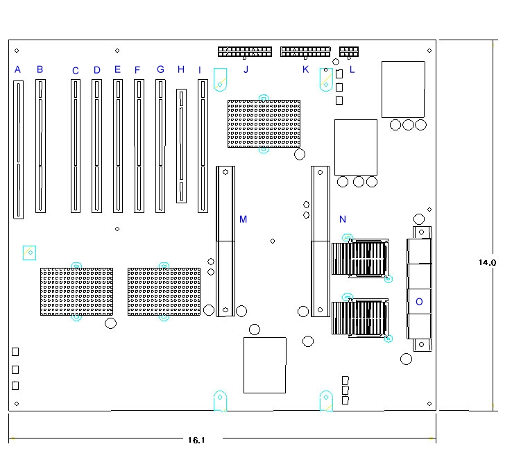
Figure 14. Baseboard Connectors
|
A. |
I/O Board Connector |
I. |
PCI Slot 6 |
|
B. |
PCI Slot 7 (S2) |
J. |
24-pin power connector |
|
C. |
PCI Slot 1 |
K. |
22-pin power connector |
|
D. |
PCI Slot 2 |
L. |
8-pin power connector |
|
E. |
PCI Slot 3 |
M. |
Memory board connector 1 |
|
F. |
PCI Slot 4 |
N. |
Memory board connector 2 |
|
G. |
PCI Slot 5 |
O. |
Processor board connector |
|
H. |
AGP Connector |
The baseboard has two- (2), 64-bit PCI buses contained in two- (2), PCI segments:
/
NOTEAll PCI buses support 64-bit, 33 MHz PCI cards and are 5V tolerant.
AGP 4x @ 50 MHz is active but not fully validated.
An ATI Rage Pro 128 add-in PCI card provides video on the Workstation SDV system. Other video devices, whether PCI- or AGP-based, are not supported.
The Workstation SDV system has aIncludes one Qlogic* 1280 PCI based SCSI controller card that fits into a PCI Slot.
IDE is a 16-bit interface for integrated disk drives with AT
* disk controller electronics onboard. The IFB (I/O and Firmware Bridge) is a multifunction device on the I/O Board that acts as a PCI-based Fast IDE controller. The device controls:
The PS/2-compatible keyboard and mouse connectors are mounted in a single-stacked housing with the mouse connector over the keyboard. External to the system, they appear as two- (2) connectors.
As viewed from the rear of the system, the keyboard connector plugs into the left PS/2 connector and the mouse plugs into the PS/2 connector on the right. Refer to Table 4.
The chassis front panel includes:
/
NOTEThe front panel USB and audio connectors are not functional on the Workstation SDV system.
(This Page Left Intentionally Blank)
This system uses an Intel-proprietary BIOS, which is stored on the 82802AC FWH and can be upgraded using a disk-based program. Table 7 provides an overview of the features supported by the beta Workstation SDV BIOS.
/
NOTEThe EFI Shell displays a message during that identifies the type of BIOS and a revision code. See
Figure 6.
Table 7. Workstation BoardSDV BIOS Features
|
Feature |
Description |
|
BIOS Upgrades |
Due to the the large file size of the SDV BIOS image (in excess of 3.75 MB) Flash memory upgrades of the BIOS requires uses LS-120 media. The BETA SDV workstation incorporates an A2 stepping of the processor, when downloading the BIOS image from the premier support web site (https://premier.intel.com) Select the BIOS build and PAL (processor abstraction layer) appropriate for A2 stepping processors |
|
Enhanced IDE |
|
|
ATAPI |
|
|
Video Support |
Supports ATI Rage Pro* 128 PCI graphics card |
|
Available Language |
English (U.S.) |
|
Boot Options |
SCSI Support has been added to the Workstation SDV |
|
USB |
Is Not Supported by the system in BIOS and the system hardware, however OS specific drivers are required or OS at this time |
|
BIOS Recovery |
Recovery is will be available in Beta timeframe |
BIOS Flash Memory Organization
The Intel* E82802AC Firmware Hub (FWH) includes an 8 Mbit (1024 KB) symmetrical flash memory device. There are four- (4), FWH devices located on the I/O Board for a total of 4 MB of flash memory. Internally, each device is grouped into eight- (8), 64-KB blocks that are individually erasable, lockable, and unlockable with additional hardware protection for the top block.
Plug and Play: PCI Auto-configuration
Minimal testing has been done on the PCI Auto-configuration for the Workstation SDV System.
IDE support is fixed configuration on Workstation SDV systems. This is expanded to ATAPI devices; no IDE drives are shipped with the system.
System Management BIOS (SMBIOS)
SMBIOS is a Desktop Management Interface (DMI) compliant methodology used for managing computers in a managed network. SMBIOS is not supported on Workstation SDV systems.
The following section describes how to upgrade the System BIOS.
Before you upgrade the BIOS, prepare by:
Obtaining the BIOS Upgrade File
You can upgrade to a new version of the BIOS by using the BIOS upgrade file. The BIOS upgrade file is a compressed, self-extracting archive that contains all the files you need to upgrade the BIOS.
You can obtain the BIOS upgrade file from the Intel Premier Support web site:
https://premier.intel.com. A login and password is required for this secure web site. You can apply for access to the Premier Support web site by going to http://support.intel.com/support/go/ItaniumSDV. Contact your Intel field representative if you need help obtaining access to this web site.
/
NOTEPlease review the instructions distributed with the BIOS files for any last minute notes before attempting a BIOS upgrade.
Creating the BIOS Upgrade Diskette
To create a BIOS upgrade or recovery diskette, do the following:
IFlash64 for Workstation SDV Release Notes
Copyright (c) 1999 Intel Corporation
All Rights Reserved
October 22, 1999
The IFlash64 utility is an EFI application program
used for updating the BIOS for Workstation SDV systems.
NOTE: This is the same app used for the Server SDV with a few minor modifications.
RELEASE NOTES FOR IFLASH64 VERSION 0.1 *RC*
A. IFLASH64 CHANGES SINCE PREVIOUS VERSION
- Default base has been changed to 0xFFC00000 from 0xFFD00000
- Fix to chipset errata regarding bit 15 in the LPC enable register.
B. DEPENDENCIES
* Executes under the EFI Shell Ver 0.91 or greater
* Binary input file must be in increments of 1MB
C. HOW TO USE THIS UTILITY
1. Boot to EFI shell.
2. Copy IFlash64.EFI and binary input file to a LS120 disk.
3. Enter the following command line and follow screen instructions:
IFlash64 [File Name] /a=0
4. Reboot system after the update is competed.
D. ADDITIONAL NOTES
1. IFlash64 programs the FLASH from address 0xFFC00000
2. IFlash64 only programs and erases the amount of FLASH required
for the update; this is determined by the size of the file.
3. Additional information can be obtained from the utility help command:
IFlash64 /h
E
. TOOLS USED IN BUILD1. IA64 SDK Tools
2. EFI
(end)
Use the following procedure to upgrade the BIOS:
_____________________________________
UPGRADING THE SYSTEM BIOS
CREATING A BIOS UPGRADE DISKETTE:
Use a newly formatted disk.
The BIOS recovery feature is not available on Workstation SDV systems.
Only American English is supported on the Workstation SDV systems.
SCSI HDD Boot is available.
During the POST, the BIOS utility generates diagnostic progress codes (POST-codes) to I/O ports 80h and 81h. If the POST fails, execution stops and the last POST-code generated is left at ports 80h and 81h. These codes are useful for determining the point where an error occurred.
Displaying the POST-codes requires an add-in card (often called a POST card). The POST card can decode the port and display the contents on a medium such as a seven-segment display.
Refer to Table 8 for descriptions of the POST-codes generated by the BIOS.
POST Codes Testing Phase
BIOS indicates the current testing phase during POST after the video adapter has been successfully initialized by outputting a 2-digit hex code to I/O location 80h. To view POST-codes, you must install an optional PCI POST add-in board. For more information, contact your designated Intel or Premier Support Site representative.
/
NOTEPort 0x81 of the POST-codes is currently only used for debug purposes.
|
Table 8. POST Codes |
|||
|
POST code (port 0x80 ) |
POST code (port 0x81) |
Beep |
Descriptions |
|
01 |
Enter memory configuration transition state |
||
|
01 |
Configure SAC memory address space |
||
|
02 |
Configure PXB0 for memory address TOM and base |
||
|
03 |
Configure PXB1 for memory address TOM and base |
||
|
04 |
Configure F16s for IO space |
||
|
05 |
Configure memory mode, refresh rate, and cache size |
||
|
06 |
Configure DRAM information and population |
||
|
07 |
Configure memory ranges |
||
|
08 |
Configure memory addresses |
||
|
09 |
Configure memory sizes |
||
|
0a |
Configure memory rows |
||
|
0b |
Begin memory auto initialization |
||
|
0c |
Execute memory reset for both memory cards |
||
|
0d |
Enable memory range from 80000h to effffh for R/W access |
||
|
02 |
Enter PID configuration transition state |
||
|
10 |
Configure PID SAPIC mode and memory map address |
||
|
11 |
Set I2BMST bit and enable serial IRQs bits for IRQ[1,4,12] |
||
|
12 |
Configure PCI mappings for INTIOs, INTIOs and serial IRQs |
||
|
13 |
Enable INTIO IRQs |
||
|
14 |
Enable Serial IRQ global and INTIO IRQ global |
||
|
15 |
Enable PID as a master for SAPIC mode |
||
|
16 |
Configure PID GPIOs |
||
|
03 |
Enter IFB configuration transition state |
||
|
20 |
Configure IFB flash access to 4MB |
||
|
21 |
Program special cycle, XBCS, DMA, deterministic and master latency timer |
||
|
22 |
Configure ACPI base address |
||
|
23 |
Configure IFB GPIO base address and initialization |
||
|
24 |
Program IDE |
||
|
25 |
Configure IRQ interrupt routings |
||
|
26 |
Configure LPC |
||
|
27 |
Configure SMBus |
||
|
28 |
Configure USB |
||
|
29 |
Enable 8259 initialization mode |
||
|
04 |
Enter SIO transition state |
||
|
3A |
set SIO GPIO attributes for address base configuration |
||
|
3B |
set SIO GPIO attributes for GPIO10-17 |
||
|
3C |
set SIO GPIO attributes for GPIO20-27 |
||
|
3D |
set SIO GPIO attributes for GPIO30-37 |
||
|
3E |
set SIO GPIO attributes for GPIO40-43 |
||
|
3F |
set SIO GPIO attributes for GPIO50-57 |
||
|
40 |
set SIO GPIO attributes for GPIO60-61 |
||
|
41 |
set initial values for SIO GPIOs (input, output, LED) |
||
|
42 |
SIO – FDD |
||
|
43 |
SIO – Parallel Port |
||
|
44 |
SIO – Serial Port #1 |
||
|
45 |
SIO – Serial Port #2 / DMA |
||
|
46 |
SIO – Keyboard |
||
|
47 |
SIO – Game Port |
||
|
48 |
SIO – MPU |
||
|
49 |
SIO – exit config. |
||
(This Page Left Intentionally Blank)
This chapter helps you identify and solve problems that might occur while you are using the beta Workstation SDV system.
|
To do this: |
Press: |
|
Soft boot reset, which clears system memory and reloads the operating system. |
<Ctrl+Alt+Del> |
|
Cold boot reset, which clears system memory, restarts POST, and initializes halts power to all all peripherals. Hold the power button for 4 seconds to Power off. Hard reset, which also clears system memory, restarts POST, and initializes all peripherals. |
Power off/on Press the reset switch located on a card slot filler panel at the rear of the system |
Incorrect installation or configuration usually causes problems that occur at initial system startup. Hardware failure is a less frequent cause.
c
Is at least one- (1) memory board installed and fully seated?
/
NOTEIf these items are correct but the problem still reoccurs contact Intel Customer Support by calling 1-800-628-8686 then pressing the 672, extension code. Outside the U.S. and Canada, call 1+503-696-6012. Or, go to
http://support.intel.com/support/go/ItaniumSDV.
Review the Post-code section that starts on page 38 again, before proceeding.
/
NOTEA Post card is required to view POST- codes.
Verifying Proper Operation of Key System Lights
As POST determines the system configuration, it tests for the presence of each mass-storage device installed in the system. As each device is checked, its activity light should turn on briefly.
Check for the following:
If you have network problems, consult the documentation for the D101 Ethernet card that was supplied with the system.
Some common PCI installation tips:
/
NOTEPCI peripherals will not operate if used with IA-32 drivers.
At this time, there are a limited number of drivers available for IA-64 PCI peripherals, do not install any additional PCI peripherals that do not have current IA-64 drivers.
Error and Informational Messages
When you turn on the system, POST displays messages that provide information about the system.
NOTE
POST beep codes and error messages are not functional on Workstation SDV systems.
Specific Problems and Corrective Actions
This section provides possible solutions for these specific problems:
Try the solutions in the order given. If you cannot correct the problem, contact Intel Customer Support or the Premier Support web site.
Check the following:
/
NOTEIf these items are correct but the problem still reoccurs contact Intel Customer Support by calling 1-800-628-8686 then pressing the 672 extension code. Outside the U.S. and Canada, call 1+503-696-6012. Or, go to
http://support.intel.com/support/go/ItaniumSDV.
Check the following:
/
NOTEBooting to the EFI prompt on a SDV Workstation takes approximately 90 seconds even with CACHE enabled.
No Characters Appear on the Screen
Check the following:
Characters Are Distorted or Incorrect
Check the following:
If the problem persists, the video monitor may be faulty or it may be the incorrect type. Contact the service representative for the monitor for assistance.
System Cooling Fans Do Not Rotate Properly
If the system cooling fans are not operating properly, system components could be damaged.
Check the following:
/
NOTEIf the failure symptoms persist please contact Intel Customer Support by calling 1-800-628-8686 then pressing the 672 extension code. Outside the U.S. and Canada, call 1+503-696-6012. Or, go to
http://support.intel.com/support/go/ItaniumSDV.
LS-120 Drive Activity Light Does Not Light or drive is not detected
Check the following:
/
NOTEIf the problem persists, there may be a problem with the LS-120 drive, I/O Board, or drive signal cable. Contact Intel Customer Support by calling 1-800-628-8686 then pressing the 672 extension code. Outside the U.S. and Canada, call 1+503-696-6012. Or, go to
http://support.intel.com/support/go/ItaniumSDV. .
Hard Disk Drive Activity Light Does Not Light
If hard disk drive activity light does not function, check the following:
/
NOTEThe front panel hard disk LED indicates IDE disk and SCSI device activity:
The hard disk drive activity light on the front panel lights when either an IDE hard disk drive, or a SCSI device is accessed. This LED does not display IDE CD-ROM drive activity.
CD-ROM Drive Activity Light Does Not Light
Check the following:
/
NOTEThe front panel hard disk LED indicates IDE disk and SCSI device activity:
The hard disk drive activity light on the front panel lights when either an IDE hard disk drive, or a SCSI device is accessed. This LED does not display IDE CD-ROM drive activity.
A speaker is mounted on the chassis but is currently not enabled by the BIOS
POST beep codes and audible error messages are not functional on Workstation SDV systems.
If you have network problems, consult the documentation for the D101 Ethernet card that was supplied with the system.
Some common PCI tips are listed here.
/
NOTEPCI peripherals will not operate if used with IA-32 drivers.
At this time, there are a limited number of drivers available for IA-64 PCI peripherals, do not install any additional PCI peripherals that do not have current IA-64 drivers.
Bootable CD-ROM Is Not Detected
Check the following:
Is BIOS set to allow the CD-ROM to be the first bootable device?
/
NOTECD-ROM Bootstrap is not functional on the Workstation SDV.
Error and Informational Messages
When you turn on the system, a POST card can display messages that provide information about the system. A POST card must be installed in a connector on PCI Bus 0 (PCI connectors 5, 6 or 7 (S2). Refer Figure 14.
(This Page Is Left Intentionally Blank)
This section describes the connectors on the Workstation SDV Beta board set. The board set is composed of a processor board, a Baseboard, two- (2) Memory boards, and an I/O board.
This section includes:
Processor Board Connectors
|
Pin |
Signal Name |
Pin |
Signal Name |
|
1 |
VCX |
14 |
TRST# |
|
2 |
TGND |
15 |
RST |
|
3 |
BPM[0]# |
16 |
TCK |
|
4 |
DBA# |
17 |
FBO |
|
5 |
BPM[1]# |
18 |
FBI |
|
6 |
DBR# |
19 |
BCLKp |
|
7 |
BPM[2]# |
20 |
TGND |
|
8 |
TGND |
21 |
BCLKn |
|
9 |
BPM[3]# |
22 |
PWR |
|
10 |
TDI |
23 |
BPM5dr |
|
11 |
BPM[4]# |
24 |
TDO |
|
12 |
TMS |
25 |
TGND |
|
13 |
BPM[5]# |
26 |
VCX |
|
H |
G |
F |
E |
D |
C |
B |
A |
|
|
1 |
GND |
RSP* |
PICCLK |
RS1* |
GND |
BR1* |
GND |
BR0* |
|
2 |
THRMALERT0* |
DBSY* |
GND |
RP* |
THRMALERT1* |
REQ3* |
GND |
BINIT* |
|
3 |
GND |
DEFER* |
GND |
INIT* |
GND |
RS0* |
ITPCLKP |
HIT* |
|
4 |
GND |
ADS* |
GND |
LOCK* |
GND |
BPRI* |
GND |
RS2* |
|
5 |
SMVCC2 |
SMSC |
GND |
REQ4* |
GND |
HITM* |
ITPCLKN |
REQ0* |
|
6 |
SMVCC1 |
SMSD |
GND |
REQ2* |
GND |
REQ1* |
GND |
BERR* |
|
7 |
GND |
BNR* |
GND |
RESET* |
GND |
FERR* |
GND |
PWRGOOD |
|
8 |
PICD0 |
BPM5* |
GND |
DRDY* |
GND |
IGNNE* |
GND |
PMI* |
|
9 |
PICD1 |
BPM4* |
GND |
LINT0 |
GND |
LINT1 |
GND |
IDS* |
|
10 |
GND |
BPM3* |
Reserved |
PPODGD0 |
GND |
AP0* |
GND |
ID6* |
|
11 |
GND |
BPM2* |
Reserved |
PPODGD1 |
GND |
AP1* |
GND |
ID5* |
|
12 |
GND |
BPM1* |
GND |
A3* |
GND |
A20M* |
GND |
ID3* |
|
13 |
GND |
BPM0* |
GND |
A5* |
GND |
A4* |
GND |
ID2* |
|
14 |
GND |
TDI |
GND |
A8* |
GND |
A6* |
GND |
ID4* |
|
15 |
GND |
TRST* |
GND |
A10* |
GND |
A7* |
GND |
ID1* |
|
16 |
GND |
TRDY* |
GND |
A14* |
GND |
A9* |
GND |
ID0* |
|
17 |
GND |
TMS |
GND |
A15* |
GND |
A11* |
GND |
SBSY* |
|
18 |
GND |
TND* |
GND |
A16* |
VTT |
A13* |
GND |
EXRESET* |
|
19 |
GND |
PROCPRS0* |
GND |
A17* |
GND |
A25* |
GND |
TDO |
|
20 |
GND |
PROCPRS1* |
GND |
A12* |
VTT |
A24* |
GND |
TCK |
|
21 |
GND |
THRMTRIP0* |
GND |
A19* |
GND |
A27* |
GND |
GND |
|
22 |
GND |
TRI_ST0* |
GND |
A20* |
VTT |
A26* |
GND |
D30* |
|
23 |
GND |
THRMTRIP1* |
GND |
A21* |
GND |
A29* |
GND |
D31* |
|
24 |
GND |
TRI_ST1* |
GND |
A22* |
VTT |
A31* |
GND |
D28* |
|
25 |
GND |
VREFAC0 |
GND |
A23* |
GND |
A30* |
GND |
D29* |
|
26 |
GND |
VREFD1 |
GND |
A18* |
VTT |
A28* |
GND |
D26* |
|
27 |
GND |
VREFD0 |
GND |
A35* |
GND |
A33* |
GND |
D27* |
|
28 |
GND |
GND |
GND |
A34* |
VTT |
A32* |
GND |
D16* |
|
29 |
GND |
D14* |
GND |
D32* |
GND |
D48* |
GND |
D17* |
|
30 |
GND |
D15* |
GND |
D33* |
VTT |
D49* |
GND |
DEP2* |
|
31 |
GND |
D12* |
GND |
D34* |
GND |
D50* |
GND |
D24* |
|
32 |
GND |
D13* |
GND |
D35* |
VTT |
D51* |
GND |
D25* |
|
33 |
GND |
D10* |
GND |
D36* |
GND |
D52* |
GND |
DEP3* |
|
34 |
GND |
D11* |
GND |
D37* |
VTT |
D53* |
GND |
STBP1* |
|
35 |
GND |
D8* |
GND |
D39* |
GND |
D54* |
GND |
STBN1* |
|
36 |
GND |
D9* |
GND |
D38* |
VTT |
D55* |
GND |
D19* |
|
37 |
GND |
STBP0* |
GND |
DEP4* |
GND |
STBP3* |
GND |
D22* |
|
38 |
GND |
STBN0* |
GND |
DEP5* |
VTT |
STBN3* |
GND |
D23* |
|
39 |
GND |
DEP0* |
GND |
STBN2* |
GND |
DEP7* |
GND |
D20* |
|
40 |
GND |
DEP1* |
GND |
STBP2* |
VTT |
DEP6* |
GND |
D21* |
|
41 |
GND |
D6* |
GND |
D40* |
GND |
D56* |
GND |
D18* |
|
42 |
GND |
D7* |
GND |
D41* |
VTT |
D57* |
GND |
GND |
|
43 |
GND |
D4* |
GND |
D42* |
GND |
D58* |
GND |
BCLKP2 |
|
44 |
GND |
D5* |
GND |
D43* |
VTT |
D59* |
GND |
BCLKN2 |
|
45 |
GND |
D2* |
GND |
D44* |
GND |
D60* |
GND |
GND |
|
46 |
GND |
D3* |
GND |
D45* |
VTT |
D61* |
GND |
BCLKP1 |
|
47 |
GND |
D0* |
GND |
D46* |
VTTSENSE |
D63* |
GND |
BCLKN1 |
|
48 |
GND |
D1* |
GND |
D47* |
VTTSENSERTN |
D62* |
GND |
GND |
Baseboard Connectors
|
A |
B |
|
|
1 |
-12V |
N/C |
|
2 |
N/C |
+12V |
|
3 |
+12V |
N/C |
|
4 |
N/C |
+12V |
|
5 |
PCI_AD0 |
N/C |
|
6 |
N/C |
PCI_AD1 |
|
7 |
+3.3V |
GND |
|
8 |
N/C |
PCI_AD3 |
|
9 |
PCI_AD2 |
PCI_AD5 |
|
10 |
PCI_AD4 |
PCI_AD7 |
|
11 |
PCI_AD6 |
N/C |
|
12 |
GND |
+5V |
|
13 |
PCI_AD8 |
N/C |
|
14 |
PCI_AD10 |
PCI_AD9 |
|
15 |
PCI_AD12 |
PCI_AD11 |
|
16 |
N/C |
PCI_AD13 |
|
17 |
+3.3V |
GND |
|
18 |
N/C |
PCI_AD15 |
|
19 |
PCI_AD14 |
PCI_AD17 |
|
20 |
PCI_AD16 |
PCI_AD19 |
|
21 |
PCI_AD18 |
N/C |
|
22 |
GND |
+5V |
|
23 |
PCI_AD20 |
N/C |
|
24 |
PCI_AD22 |
PCI_AD21 |
|
25 |
PCI_AD24 |
PCI_AD23 |
|
26 |
N/C |
PCI_AD25 |
|
27 |
+3.3V |
GND |
|
28 |
N/C |
PCI_AD27 |
|
29 |
PCI_AD26 |
PCI_AD29 |
|
30 |
PCI_AD28 |
PCI_AD31 |
|
31 |
PCI_AD30 |
N/C |
|
32 |
GND |
+5V |
|
33 |
PCI_AD32 |
N/C |
|
34 |
PCI_AD34 |
PCI_AD33 |
|
35 |
PCI_AD36 |
PCI_AD35 |
|
36 |
N/C |
PCI_AD37 |
|
37 |
+3.3V |
GND |
|
38 |
N/C |
PCI_AD39 |
|
39 |
PCI_AD38 |
PCI_AD41 |
|
40 |
PCI_AD40 |
PCI_AD43 |
|
41 |
PCI_AD42 |
N/C |
|
42 |
GND |
+5V |
|
43 |
PCI_AD44 |
N/C |
|
44 |
PCI_AD46 |
PCI_AD45 |
|
45 |
PCI_AD48 |
PCI_AD47 |
|
46 |
N/C |
PCI_AD49 |
|
47 |
+3.3V |
GND |
|
48 |
N/C |
PCI_AD51 |
|
49 |
PCI_AD50 |
PCI_AD53 |
|
50 |
PCI_AD52 |
PCI_AD55 |
|
51 |
PCI_AD54 |
N/C |
|
52 |
GND |
+5V |
|
53 |
PCI_AD56 |
N/C |
|
54 |
PCI_AD58 |
PCI_AD57 |
|
55 |
PCI_AD60 |
PCI_AD59 |
|
56 |
N/C |
PCI_AD61 |
|
57 |
+3.3V |
GND |
|
58 |
N/C |
PCI_AD63 |
|
59 |
PCI_AD62 |
C/BE4_N |
|
60 |
PCI_AD64 |
C/BE5_N |
|
61 |
C/BE0_N |
N/C |
|
62 |
GND |
+5V |
|
63 |
C/BE1_N |
N/C |
|
64 |
C/BE2_N |
C/BE6_N |
|
65 |
C/BE3_N |
C/BE7_N |
|
66 |
N/C |
REQ64_0_N |
|
67 |
+3.3V |
GND |
|
68 |
N/C |
REQ64_1_N |
|
69 |
REQ0_N |
WSC_N |
|
70 |
REQ1_N |
GNT64_0_N |
|
71 |
GNT0_N |
N/C |
|
72 |
GND |
+5V |
|
73 |
GNT1_N |
N/C |
|
74 |
TDP1 |
GNT64_1_N |
|
75 |
TDN1 |
TDP2 |
|
76 |
N/C |
TDN2 |
|
77 |
+3.3V |
GND |
|
78 |
N/C |
PAR64 |
|
79 |
PAR |
TRDY_N |
|
80 |
IRDY_N |
A20GATE |
|
81 |
N/C |
N/C |
|
82 |
+3.3V |
+5V |
|
83 |
STBY3V |
STBY5V |
|
84 |
STBY3V |
STBY5V |
|
85 |
STBY3V |
STBY5V |
|
86 |
STBY3V |
STBY5V |
|
87 |
+3.3V |
+5V |
|
88 |
N/C |
N/C |
|
89 |
FRAME_N |
DEVSEL_N |
|
90 |
STOP_N |
SERR_N |
|
91 |
PCI_PME_N |
N/C |
|
92 |
GND |
+5V |
|
93 |
PERR_N |
N/C |
|
94 |
LOCK_N |
SERIRQ |
|
95 |
CLKRUN |
A20M_N |
|
96 |
N/C |
PIRQA_N |
|
97 |
+3.3V |
GND |
|
98 |
N/C |
PIRQB_N |
|
99 |
IGNNE |
PIRQC_N |
|
100 |
INTR |
PIRQD_N |
|
101 |
NMI |
N/C |
|
102 |
GND |
+5V |
|
103 |
SMBCLK |
N/C |
|
104 |
SMBDATA |
CPU_SMI_N |
|
105 |
SMBALERT_N |
PHOLD_N |
|
106 |
N/C |
PHOLDA_N |
|
107 |
+3.3V |
GND |
|
108 |
N/C |
CPU_PRESO_N |
|
109 |
APICD0 |
CPU_PRES1_N |
|
110 |
APICD1 |
FERR_N |
|
111 |
ECCINT_N |
N/C |
|
112 |
GND |
+5V |
|
113 |
SUSTAT_N |
N/C |
|
114 |
SLP_S(3) |
AUX_PWR_OK |
|
115 |
SLP_S(5) |
PWR_GOOD |
|
116 |
N/C |
PWR_BTN |
|
117 |
+3.3V |
GND |
|
118 |
N/C |
IRQ(1) |
|
119 |
INIT_N |
IRQ(3) |
|
120 |
IRQ(4) |
|
|
121 |
FP_RESET_N |
N/C |
|
122 |
GND |
+5V |
|
123 |
PCIRST_N |
N/C |
|
124 |
IRQ(5) |
|
|
125 |
KYBD_RST_N |
IRQ(6) |
|
126 |
N/C |
IRQ(7) |
|
127 |
+3.3V |
GND |
|
128 |
N/C |
IRQ(9) |
|
129 |
IRQ(10) |
IRQ(11) |
|
130 |
IRQ(12) |
IRQ(14) |
|
131 |
IRQ(15) |
N/C |
|
132 |
GND |
+5V |
|
133 |
APC_ONCNTRL |
N/C |
|
134 |
IDRAM_PRSNT_N |
FEMPTY_N |
|
135 |
IO_PRSNT_N |
m |
|
136 |
N/C |
|
|
137 |
+3.3V |
GPIO_1 |
|
138 |
N/C |
GND |
|
139 |
GPIO_0 |
GPIO_3 |
|
140 |
GPIO_2 |
GPIO_5 |
|
141 |
GPIO_4 |
GPIO_7 |
|
142 |
GPIO_8 |
GPIO_11 |
|
143 |
GPIO_10 |
N/C |
|
144 |
N/C |
+5V |
|
145 |
+3.3V |
N/C |
|
146 |
N/C |
GPIO_13 |
|
147 |
GPIO_12 |
IRQ(21) / GPIO_15 |
|
148 |
IRQ(20) / GPIO_14 |
IRQ(23) / GPIO_17 |
|
149 |
IRQ(22) / GPIO_16 |
GPIO_19 |
|
150 |
GPIO_18 |
GPIO_21 |
|
151 |
GPIO_20 |
GPIO_22 |
|
152 |
GND |
GND |
|
153 |
APIC_CLK |
SUSCLK |
|
154 |
GND |
GND |
|
155 |
LCLK0 |
LCLK1 |
|
156 |
GND |
GND |
|
157 |
LCLK2 |
LCLK3 |
|
158 |
GND |
GND |
|
159 |
AUDIO_CLK |
OSC(14.318MHZ) |
|
160 |
GND |
GND |
|
161 |
USB_CLK_0 |
USB_CLK_1 |
|
162 |
GND |
GND |
|
163 |
PCI_CLK_0 |
PCI_CLK_1 |
|
164 |
GND |
GND |
|
165 |
PCI_CLK_2 |
PCI_CLK_3 |
|
166 |
GND |
GND |
|
167 |
FWH_CLK_0 |
FWH_CLK_1 |
|
168 |
GND |
GND |
|
169 |
FWH_CLK_2 |
FWH_CLK_3 |
|
170 |
GND |
GND |
|
Pin# |
D |
C |
|
1 |
VCC3.3 |
Ground |
|
2 |
VCC3.3 |
VCC3.3 |
|
3 |
VCC3.3 |
Ground |
|
4 |
VCC3.3 |
VCC3.3 |
|
5 |
VCC3.3 |
Ground |
|
6 |
VCC3.3 |
Ground |
|
7 |
VCC3.3 |
Ground |
|
8 |
VCC3.3 |
Ground |
|
9 |
PRSNT2# |
Reserved |
|
10 |
PRSNT1# |
Reserved |
|
F |
E |
|
|
1 |
Reserved |
Reserved |
|
2 |
Reserved |
Reserved |
|
3 |
Ground |
VCC12 |
|
4 |
Ground |
VCC12 |
|
5 |
Ground |
VCC12 |
|
6 |
Ground |
VCC12 |
|
7 |
Ground |
VCC12 |
|
8 |
Ground |
VCC12 |
|
9 |
Ground |
VCC12 |
|
10 |
Ground |
VCC12 |
|
11 |
Ground |
VCC12 |
|
12 |
Ground |
VCC12 |
|
13 |
Ground |
VCC12 |
|
14 |
Ground |
VCC12 |
Note:
Pins A1–A66 and B1–B66 are same as for the AGP connector|
Pin# |
B |
A |
|
1 |
OVRCNT# |
12V |
|
2 |
5.0V |
Reserved |
|
3 |
5.0V |
TYPEDET# |
|
4 |
USB+ |
USB- |
|
5 |
GND |
GND |
|
6 |
INTB# |
INTA# |
|
7 |
CLK |
RST# |
|
8 |
REQ# |
GNT# |
|
9 |
VCC3.3 |
VCC3.3 |
|
10 |
ST0 |
ST1 |
|
11 |
ST2 |
Reserved |
|
12 |
RBF# |
PIPE# |
|
13 |
GND |
GND |
|
14 |
Reserved |
WBF# |
|
15 |
SBA0 |
SBA1 |
|
16 |
VCC3.3 |
VCC3.3 |
|
17 |
SBA2 |
SBA3 |
|
18 |
SB_STB |
SB_STB# |
|
19 |
GND |
GND |
|
20 |
SBA4 |
SBA5 |
|
21 |
SBA6 |
SBA7 |
|
22 |
Reserved |
Reserved |
|
23 |
GND |
GND |
|
24 |
Reserved |
Reserved |
|
25 |
VCC3.3 |
VCC3.3 |
|
26 |
AD31 |
AD30 |
|
27 |
AD29 |
AD28 |
|
28 |
VCC3.3 |
VCC3.3 |
|
29 |
AD27 |
AD26 |
|
30 |
AD25 |
AD24 |
|
31 |
GND |
GND |
|
32 |
AD_STB1 |
AD_STB1# |
|
33 |
AD23 |
C/BE3# |
|
34 |
Vddq |
Vddq |
|
35 |
AD21 |
AD22 |
|
36 |
AD19 |
AD20 |
|
37 |
GND |
GND |
|
38 |
AD17 |
AD18 |
|
39 |
C/BE2# |
AD16 |
|
40 |
Vddq |
Vddq |
|
41 |
IRDY# |
FRAME# |
|
42 |
Reserved |
Reserved |
|
43 |
GND |
GND |
|
44 |
Reserved |
Reserved |
|
45 |
VCC3.3 |
VCC3.3 |
|
46 |
DEVSEL# |
TRDY# |
|
47 |
Vddq |
STOP# |
|
48 |
PERR# |
PME# |
|
49 |
GND |
GND |
|
50 |
SERR# |
PAR |
|
51 |
C/BE1# |
AD15 |
|
52 |
Vddq |
Vddq |
|
53 |
AD14 |
AD13 |
|
54 |
AD12 |
AD11 |
|
55 |
GND |
GND |
|
56 |
AD10 |
AD9 |
|
57 |
AD8 |
C/BE0# |
|
58 |
Vddq |
Vddq |
|
59 |
AD_STB0 |
AD_STB0# |
|
60 |
AD7 |
AD6 |
|
61 |
GND |
GND |
|
62 |
AD5 |
AD4 |
|
63 |
AD3 |
AD2 |
|
64 |
Vddq |
Vddq |
|
65 |
AD1 |
AD0 |
|
66 |
Reserved |
Reserved |
|
Pin |
Signal Name |
|
1 |
Tach Out |
|
2 |
+12V |
|
3 |
Fan Enable |
|
Pin |
Signal Name |
|
1 |
Internal thermistor |
|
2 |
To Speed Circuit |
|
3 |
External thermistor |
|
Signal Name |
Pin |
Signal Name |
Pin |
Signal Name |
Pin |
Signal Name |
Pin |
|
D63# |
AF38 |
A03# |
K12 |
ID5# |
AN29 |
3.3V |
A1 |
|
D62# |
AD38 |
A04# |
H12 |
ID6# |
AM28 |
3.3V |
B2 |
|
D61# |
AF36 |
A05# |
F12 |
ID7# |
AN27 |
TUNER1 |
AK2 |
|
D60# |
AD36 |
A06# |
D12 |
IDS# |
AM26 |
TUNER2 |
AH2 |
|
D59# |
AF34 |
A07# |
K14 |
IERR |
K6 |
VCCMON |
A9 |
|
D58# |
AD34 |
A08# |
H14 |
IGNNE# |
D8 |
VSBL# |
AM18 |
|
D57# |
AF32 |
A09# |
F14 |
INIT# |
AN7 |
VSSMON |
A7 |
|
D56# |
AD32 |
A10# |
D14 |
LINT0 |
F8 |
VREF |
L19 |
|
DEP6# |
AF30 |
A11# |
B14 |
LINT1 |
E9 |
VREF |
L23 |
|
STBN3# |
AD28 |
A12# |
A15 |
LOCK# |
AF16 |
VREF |
L27 |
|
STBP3# |
AF28 |
A13# |
K16 |
LYA0 |
AN1 |
VREF |
L30 |
|
DEP7# |
AD30 |
A14# |
H16 |
LYA1 |
AJ1 |
VREF |
AC19 |
|
D55# |
AF26 |
A15# |
F16 |
NCBPCLK2 |
L7 |
VREF |
AC23 |
|
D54# |
AD26 |
A16# |
D16 |
NCBPCLK3 |
K8 |
VREF |
AC27 |
|
D53# |
AF24 |
A17# |
B17 |
NCBYPASS |
AN3 |
VREF |
AC31 |
|
D52# |
AD24 |
A18# |
A17 |
NCCRVS0 |
B8 |
VTT |
E3 |
|
D51# |
AF22 |
A19# |
K18 |
NCCRVS1 |
C9 |
VTT |
E7 |
|
D50# |
AD22 |
A20# |
H18 |
NCCRVS2 |
G9 |
VTT |
E19 |
|
D49# |
AF20 |
A21# |
F18 |
NCCRVS3 |
AD8 |
VTT |
E23 |
|
D48# |
AD20 |
A22# |
D18 |
NCCRVS4 |
AF8 |
VTT |
E27 |
|
D47# |
AK38 |
A23# |
A18 |
NCCRVS5 |
AH8 |
VTT |
G19 |
|
D46# |
AH38 |
A24# |
B20 |
NCCRVS6 |
AK8 |
VTT |
G23 |
|
D45# |
AK36 |
A25# |
A19 |
NCCRVS7 |
AM8 |
VTT |
G27 |
|
D44# |
AH36 |
A26# |
B22 |
NCRSV0 |
D6 |
VTT |
J3 |
|
D43# |
AK34 |
A27# |
A21 |
NCRSV1 |
H6 |
VTT |
J7 |
|
D42# |
AH34 |
A28# |
B24 |
NCRSV2 |
AH4 |
VTT |
J19 |
|
D41# |
AK32 |
A29# |
A23 |
NCRSV3 |
AK4 |
VTT |
J23 |
|
D40# |
AH32 |
A30# |
B26 |
NCRSV4 |
AM4 |
VTT |
J27 |
|
DEP4# |
AH28 |
A31# |
A25 |
NC(TDI) |
A5 |
VTT |
AE3 |
|
STBN2# |
AK30 |
A32# |
B28 |
OUTEN |
AM2 |
VTT |
AE7 |
|
STBP2# |
AH30 |
A33# |
A27 |
PICCLK |
AC7 |
VTT |
AE19 |
|
DEP5# |
AK28 |
A34# |
B30 |
PiCD0 |
AD4 |
VTT |
AE23 |
|
D39# |
AH26 |
A35# |
A29 |
PiCD1 |
AF4 |
VTT |
AE27 |
|
D38# |
AK26 |
A36# |
B32 |
PMI# |
AG7 |
VTT |
AG19 |
|
D37# |
AK24 |
A37# |
A31 |
PPODGD |
AL3 |
VTT |
AG23 |
|
D36# |
AH24 |
A38# |
B34 |
PROCPRES# |
A3 |
VTT |
AG27 |
|
D35# |
AK22 |
A39# |
A33 |
PWRGOOD |
AN5 |
VCT |
AJ3 |
|
D34# |
AH22 |
A40# |
B36 |
RESET# |
AM16 |
VCT |
AJ7 |
|
D33# |
AK20 |
A41# |
A35 |
REQ0# |
AH16 |
VCT |
AJ19 |
|
D32# |
AH20 |
A42# |
B38 |
REQ1# |
AC17 |
VCT |
AJ23 |
|
D31# |
D20 |
A43# |
A37 |
REQ2# |
AK14 |
NC |
B6 |
|
D30# |
F20 |
32/64B |
AJ5 |
REQ3# |
AF12 |
NC |
E4 |
|
D29# |
D22 |
A20M# |
H8 |
REQ4# |
AD14 |
NC |
G3 |
|
D28# |
F22 |
AP0# |
B12 |
RP# |
AK12 |
NC |
J5 |
|
D27# |
D24 |
AP1# |
A13 |
RS0# |
AH14 |
NC |
AC3 |
|
D26# |
F24 |
ADS# |
AF18 |
RS1# |
AM12 |
NC |
AD2 |
|
D25# |
D26 |
BCKLP |
AM38 |
RS2# |
AF14 |
NC |
AE1 |
|
D24# |
F26 |
BCKLN |
AN37 |
RSP# |
AH12 |
NC |
AE5 |
|
DEP3# |
F28 |
BINIT# |
AM14 |
SBSY# |
AN34 |
NC |
AF2 |
|
STBP1# |
F30 |
BNR# |
AH18 |
SLP# |
L2 |
NC |
AG3 |
|
STBN1# |
D30 |
BERR# |
AK18 |
SMA0 |
B4 |
||
|
DEP2# |
D28 |
BPM0# |
AN24 |
SMA1 |
C3 |
||
|
D23# |
D32 |
BPM1# |
AM23 |
SMA2 |
D3 |
||
|
D22# |
F32 |
BPM2# |
AM22 |
SMPROT |
H2 |
||
|
D21# |
D34 |
BPM3# |
AN21 |
SMRSVD |
K2 |
||
|
D20# |
F34 |
BPM4# |
AM20 |
SMSC |
F2 |
||
|
D19# |
D36 |
BPM5# |
AN19 |
SMSD |
E1 |
||
|
D18# |
F36 |
BPRI# |
AM34 |
SMWP |
D2 |
||
|
D17# |
D38 |
BR0# |
AF10 |
STPCLK# |
J2 |
||
|
D16# |
F38 |
BR1# |
AH10 |
TCK |
AM6 |
||
|
D15# |
H20 |
BR2# |
AC11 |
TDO |
AK6 |
||
|
D14# |
K20 |
BR3# |
AK10 |
TDI |
AH6 |
||
|
D13# |
H22 |
BR4# |
AM10 |
THRMDA |
E5 |
||
|
D12# |
K22 |
BR5# |
AN11 |
THRMDC |
H4 |
||
|
D11# |
H24 |
DBSY# |
AC13 |
THRMTRIP# |
F6 |
||
|
D10# |
K24 |
DEFER |
AD16 |
TMS |
AL7 |
||
|
D09# |
H26 |
DRATE# |
AM36 |
TND# |
AN25 |
||
|
D08# |
K26 |
DRDY# |
AC15 |
TRDY# |
AD18 |
||
|
DEP1# |
H30 |
FERR# |
J9 |
TRST# |
AF6 |
||
|
STBP0# |
H28 |
FRCERR |
K4 |
||||
|
STBN0# |
K28 |
FLUSH# |
AD6 |
||||
|
DEP0# |
K30 |
HIT# |
AD12 |
||||
|
D07# |
H32 |
HITM# |
AD10 |
||||
|
D06# |
K32 |
ID0# |
AN36 |
||||
|
D05# |
H34 |
ID1# |
AN33 |
||||
|
D04# |
K34 |
ID2# |
AM32 |
||||
|
D03# |
H36 |
ID3# |
AN31 |
||||
|
D02# |
K36 |
ID4# |
AM30 |
||||
|
D01# |
H38 |
||||||
|
D00# |
K38 |
||||||
|
A |
B |
C |
D |
E |
|
|
1 |
‘GND’ |
VRM1_PWRGD’ |
‘GND’ |
‘MEM_PRESENT’ |
‘GND’ |
|
2 |
MD71_N’ |
‘GND’ |
ERR_N’ |
‘GND’ |
‘GND’ |
|
3 |
‘GND’ |
MD53_N’ |
‘GND’ |
‘GND’ |
MDC3-HCLKIN_N’ |
|
4 |
MD70_N’ |
‘GND’ |
FWSL_N’ |
‘GND’ |
‘MDC3-HCLKIN’ |
|
5 |
‘GND’ |
MD52_N’ |
‘1_8V5’ |
HWMDR_N’ |
‘GND’ |
|
6 |
MD69_N’ |
‘GND’ |
FWMD_N’ |
‘GND’ |
MDC2-HCLKIN_N’ |
|
7 |
‘GND’ |
MD51_N’ |
‘GND’ |
‘GND’ |
‘MDC2-HCLKIN’ |
|
8 |
MD68_N’ |
‘GND’ |
LRMD_N’ |
‘1_8V4’ |
‘GND’ |
|
9 |
‘GND’ |
MD50_N’ |
‘GND’ |
‘GND’ |
MAC1-HCLKIN_N’ |
|
10 |
MD67_N’ |
‘GND’ |
PAR_N’ |
GND’ |
‘MAC1-HCLKIN’ |
|
11 |
‘GND’ |
MD49_N’ |
‘1_8V3’ |
HWMDL_N’ |
‘GND’ |
|
12 |
MD66_N’ |
‘GND’ |
CMPLTL_N’ |
‘GND’ |
ROW1_N’ |
|
13 |
‘GND’ |
MD48_N’ |
‘GND’ |
CMND1_N’ |
‘GND’ |
|
14 |
MD65_N’ |
‘GND’ |
CMPLTR_N’ |
‘1_8V2’ |
ROW0_N’ |
|
15 |
‘GND’ |
MD47_N’ |
‘GND’ |
MD17_N’ |
‘GND’ |
|
16 |
MD64_N’ |
‘GND’ |
CMND0_N’ |
‘GND’ |
ROW2_N’ |
|
17 |
‘GND’ |
MD46_N’ |
‘1_8V1’ |
MD16_N’ |
‘GND’ |
|
18 |
MD63_N’ |
‘GND’ |
MEMRST_N’ |
‘GND’ |
MA16_N’ |
|
19 |
‘GND’ |
MD45_N’ |
‘GND’ |
MD15_N’ |
‘GND’ |
|
20 |
MDS5_N’ |
‘GND’ |
MD35_N’ |
‘GND’ |
MA15_N’ |
|
21 |
‘GND’ |
MDS7_N’ |
‘GND’ |
MD14_N’ |
‘GND’ |
|
22 |
MDS4_N’ |
‘GND’ |
MD34_N’ |
‘GND’ |
MA14_N’ |
|
23 |
‘GND’ |
MDS6_N’ |
‘GND’ |
MD13_N’ |
‘GND’ |
|
24 |
MD62_N’ |
‘GND’ |
MD33_N’ |
‘GND’ |
MA13_N’ |
|
25 |
‘GND’ |
MD44_N’ |
‘GND’ |
MD12_N’ |
‘GND’ |
|
26 |
MD61_N’ |
‘GND’ |
MD32_N’ |
‘GND’ |
MA12_N’ |
|
27 |
‘GND’ |
MD43_N’ |
‘GND’ |
MD11_N’ |
‘GND’ |
|
28 |
MD60_N’ |
‘GND’ |
MD31_N’ |
‘GND’ |
MA11_N’ |
|
29 |
‘GND’ |
MD42_N’ |
‘GND’ |
MD10_N’ |
‘GND’ |
|
30 |
MD59_N’ |
‘GND’ |
MD30_N’ |
‘GND’ |
MA10_N’ |
|
31 |
‘GND’ |
MD41_N’ |
‘GND’ |
MD9_N’ |
‘GND’ |
|
32 |
MD58_N’ |
‘GND’ |
MD29_N’ |
‘GND’ |
MA9_N’ |
|
33 |
‘GND’ |
MD40_N’ |
‘GND’ |
MDS0_N’ |
‘GND’ |
|
34 |
MD57_N’ |
‘GND’ |
MD28_N’ |
‘GND’ |
MA8_N’ |
|
35 |
‘GND’ |
MD39_N’ |
‘GND’ |
MDS1_N’ |
‘GND’ |
|
36 |
MD56_N’ |
‘GND’ |
MD27_N’ |
‘GND’ |
MA7_N’ |
|
37 |
‘GND’ |
MD38_N’ |
‘GND’ |
MD8_N’ |
‘GND’ |
|
38 |
MD55_N’ |
‘GND’ |
MDS3_N’ |
‘GND’ |
MA6_N’ |
|
39 |
‘GND’ |
MD37_N’ |
‘GND’ |
MD7_N’ |
‘GND’ |
|
40 |
MD54_N’ |
‘GND’ |
MDS2_N’ |
NC |
MA5_N’ |
|
41 |
‘GND’ |
MD36_N’ |
‘GND’ |
MD6_N’ |
‘GND’ |
|
42 |
‘I2C1_8-SCL’ |
‘GND’ |
MD26_N’ |
‘GND’ |
MA4_N’ |
|
43 |
‘GND’ |
‘I2C1_8-SDA’ |
‘GND’ |
MD5_N’ |
‘GND’ |
|
44 |
12V12’ |
12V6’ |
MD25_N’ |
‘GND’ |
MA3_N’ |
|
45 |
12V11’ |
12V5’ |
‘GND’ |
MD4_N’ |
‘GND’ |
|
46 |
12V10’ |
12V4’ |
MD24_N’ |
‘GND’ |
MA2_N’ |
|
47 |
12V9’ |
12V3’ |
‘GND’ |
MD3_N’ |
‘GND’ |
|
48 |
12V8’ |
12V2’ |
MD23_N’ |
‘GND’ |
MA1_N’ |
|
49 |
12V7’ |
12V1’ |
‘GND’ |
MD2_N’ |
‘GND’ |
|
50 |
‘GND’ |
‘GND’ |
MD22_N’ |
‘CONN-ID’ |
MA0_N’ |
|
51 |
mac_vref18 |
‘GND’ |
‘GND’ |
MD1_N’ |
‘GND’ |
|
52 |
‘GND’ |
mdc_vref181 |
‘GND’ |
‘GND’ |
‘MAC0-HCLKIN’ |
|
53 |
‘TDI’ |
‘GND’ |
MD21_N’ |
‘GND’ |
MAC0-HCLKIN_N’ |
|
54 |
‘GND’ |
mdc vref180 |
‘GND’ |
MD0_N’ |
‘GND’ |
|
55 |
‘TDO’ |
‘GND’ |
MD20_N’ |
‘GND’ |
MDC1-HCLKIN_N’ |
|
56 |
‘GND’ |
sdc_mvref0 |
‘GND’ |
‘GND’ |
‘MDC1-HCLKIN’ |
|
57 |
‘TCK’ |
‘GND’ |
MD19_N’ |
‘SYS_PWRGD’ |
‘GND’ |
|
58 |
‘GND’ |
sdc_mvref1 |
‘GND’ |
‘GND’ |
MDC0-HCLKIN_N’ |
|
59 |
TRST_N’ |
‘GND’ |
MD18_N’ |
‘GND’ |
‘MDC0-HCLKIN’ |
|
60 |
‘TMS’ |
sac_vrefm |
‘GND’ |
VRM0_PWRGD’ |
‘GND’ |
|
A |
B |
C |
D |
E |
|
|
5V Board |
Universal Board |
3.3V Board |
|||||
|
Pin |
Side B |
Side A |
Side B |
Side A |
Side B |
Side A |
Comments |
|
1 |
-12 V |
TRST# |
-12V |
TRST# |
-12 V |
TRST# |
32-bit start |
|
2 |
TCK |
+12 V |
TCK |
+12 V |
TCK |
+12 V |
|
|
3 |
Ground |
TMS |
Ground |
TMS |
Ground |
TMS |
|
|
4 |
TDO |
TDI |
TDO |
TDI |
TDO |
TDI |
|
|
5 |
+5 V |
+5 V |
+5 V |
+5 V |
+5 V |
+5 V |
|
|
6 |
+5 V |
INTA# |
+5 V |
INTA# |
+5 V |
INTA# |
|
|
7 |
INTB# |
INTC# |
INTB# |
INTC# |
INTB# |
INTC# |
|
|
8 |
INTD# |
+5 V |
INTD# |
+5 V |
INTD# |
+5 V |
|
|
9 |
PRSNT1# |
Reserved |
PRSNT1# |
Reserved |
PRSNT1# |
Reserved |
|
|
10 |
Reserved |
+5 V |
Reserved |
+VI/O |
Reserved |
+3.3 V |
|
|
11 |
PRSNT2# |
Reserved |
PRSNT2# |
Reserved |
PRSNT2# |
Reserved |
|
|
12 |
Ground |
Ground |
KEYWAY KEYWAY |
KEYWAY KEYWAY |
3.3Vkey |
||
|
13 |
Ground |
Ground |
3.3Vkey |
||||
|
14 |
Reserved |
Reserved |
Reserved |
Reserved |
Reserved |
Reserved |
|
|
15 |
Ground |
RST# |
Ground |
RST# |
Ground |
RST# |
|
|
16 |
CLK |
+5 V |
CLK |
+VI/O |
CLK |
+3.3 V |
|
|
17 |
Ground |
GNT# |
Ground |
GNT# |
Ground |
GNT# |
|
|
18 |
REQ# |
Ground |
REQ# |
Ground |
REQ# |
Ground |
|
|
19 |
+5V |
Reserved |
+VI/O |
Reserved |
+3.3V |
Reserved |
|
|
20 |
AD[31] |
AD[30] |
AD[31] |
AD[30] |
AD[31] |
AD[30] |
|
|
21 |
AD[29] |
+3.3 V |
AD[29] |
+3.3 V |
AD[29] |
+3.3 V |
|
|
22 |
Ground |
AD[28] |
Ground |
AD[28] |
Ground |
AD[28] |
|
|
23 |
AD[27] |
AD[26] |
AD[27] |
AD[26] |
AD[27] |
AD[26] |
|
|
24 |
AD[25] |
Ground |
AD[25] |
Ground |
AD[25] |
Ground |
|
|
25 |
+3.3V |
AD[24] |
+3.3 V |
AD[24] |
+3.3 V |
AD[24] |
|
|
26 |
C/BE[3]# |
IDSEL |
C/BE[3]# |
IDSEL |
C/BE[3]# |
IDSEL |
|
|
27 |
AD[23] |
+3.3 V |
AD[23] |
+3.3 V |
AD[23] |
+3.3 V |
|
|
28 |
Ground |
AD[22] |
Ground |
AD[22] |
Ground |
AD[22] |
|
|
29 |
AD[21] |
AD[20] |
AD[21] |
AD[20] |
AD[21] |
AD[20] |
|
|
30 |
AD[19] |
Ground |
AD[19] |
Ground |
AD[19] |
Ground |
|
|
31 |
+3.3V |
AD[18] |
+3.3V |
AD[18] |
+3.3 V |
AD[18] |
|
|
32 |
AD[17] |
AD[16] |
AD[17] |
AD[16] |
AD[17] |
AD[16] |
|
|
33 |
C/BE[2]# |
+3.3 V |
C/BE[2]# |
+3.3 V |
C/BE[2]# |
+3.3 V |
|
|
34 |
Ground |
FRAME# |
Ground |
FRAME# |
Ground |
FRAME# |
|
|
35 |
IRDY# |
Ground |
IRDY# |
Ground |
IRDY# |
Ground |
|
|
36 |
+3.3 V |
TRDY# |
+3.3 V |
TRDY# |
+3.3 V |
TRDY# |
|
|
37 |
DEVSEL# |
Ground |
DEVSEL# |
Ground |
DEVSEL# |
Ground |
|
|
38 |
Ground |
STOP# |
Ground |
STOP# |
Ground |
STOP# |
|
|
39 |
LOCK# |
+3.3 V |
LOCK# |
+3.3V |
LOCK# |
+3.3V |
|
|
40 |
PERR# |
SDONE |
PERR# |
SDONE |
PERR# |
SDONE |
|
|
41 |
+3.3 V |
SBO# |
+3.3 V |
SBO# |
+3.3 V |
SBO# |
|
|
42 |
SERR# |
Ground |
SERR# |
Ground |
SERR# |
Ground |
|
|
43 |
+3.3 V |
PAR |
+3.3 V |
PAR |
+3.3 V |
PAR |
|
|
44 |
C/BE[1]# |
AD[15] |
C/BE[1]# |
AD[15] |
C/BE[1]# |
AD[15] |
|
|
45 |
AD[14] |
+3.3 V |
AD[14] |
+3.3 V |
AD[14] |
+3.3 V |
|
|
46 |
Ground |
AD[13] |
Ground |
AD[13] |
Ground |
AD[13] |
|
|
47 |
AD[12] |
AD[11] |
AD[12] |
AD[11] |
AD[12] |
AD[11] |
|
|
48 |
AD[10] |
Ground |
AD[10] |
Ground |
AD[10] |
Ground |
|
|
49 |
Ground |
AD[09] |
M66EN |
AD[09] |
M66EN |
AD[09] |
66MHz /GND |
|
50 |
KEYWAY KEYWAY |
KEYWAY KEYWAY |
Ground |
Ground |
5Vkey |
||
|
51 |
Ground |
Ground |
5Vkey |
||||
|
52 |
AD[08] |
C/BE[0]# |
AD[08] |
C/BE[0]# |
AD[08] |
C/BE[0]# |
|
|
53 |
AD[07] |
+3.3 V |
AD[07] |
+3.3 V |
AD[07] |
+3.3 V |
|
|
54 |
+3.3 V |
AD[06] |
+3.3 V |
AD[06] |
+3.3 V |
AD[06] |
|
|
55 |
AD[05] |
AD[04] |
AD[05] |
AD[04] |
AD[05] |
AD[04] |
|
|
56 |
AD[03] |
Ground |
AD[03] |
Ground |
AD[03] |
Ground |
|
|
57 |
Ground |
AD[02] |
Ground |
AD[02] |
Ground |
AD[02] |
|
|
58 |
AD[01] |
AD[00] |
AD[01] |
AD[00] |
AD[01] |
AD[00] |
|
|
59 |
+5 V |
+5 V |
+VI/O |
+VI/O |
+3.3 V |
+3.3 V |
|
|
60 |
ACK64# |
REQ64# |
ACK64# |
REQ64# |
ACK64# |
REQ64# |
|
|
61 |
+5 V |
+5 V |
+5 V |
+5 V |
+5 V |
+5 V |
|
|
62 |
+5 V |
+5 V |
+5 V |
+5 V |
+5 V |
+5 V |
32-bit end |
|
KEYWAY KEYWAY |
KEYWAY KEYWAY |
KEYWAY KEYWAY |
64-bitspacer |
||||
|
64-bitspacer |
|||||||
|
63 |
Reserved |
Ground |
Reserved |
Ground |
Reserved |
Ground |
64-bit start |
|
64 |
Ground |
C/BE[7]# |
Ground |
C/BE[7]# |
Ground |
C/BE[7]# |
|
|
65 |
C/BE[6]# |
C/BE[5]# |
C/BE[6]# |
C/BE[5]# |
C/BE[6]# |
C/BE[5]# |
|
|
66 |
C/BE[4]# |
+5 V |
C/BE[4]# |
+VI/O |
C/BE[4]# |
+3.3 V |
|
|
67 |
Ground |
PAR64 |
Ground |
PAR64 |
Ground |
PAR64 |
|
|
68 |
AD[63] |
AD[62] |
AD[63] |
AD[62] |
AD[63] |
AD[62] |
|
|
69 |
AD[61] |
Ground |
AD[61] |
Ground |
AD[61] |
Ground |
|
|
70 |
+5 V |
AD[60] |
+VI/O |
AD[60] |
+3.3 V |
AD[60] |
|
|
71 |
AD[59] |
AD[58] |
AD[59] |
AD[58] |
AD[59] |
AD[58] |
|
|
72 |
AD[57] |
Ground |
AD[57] |
Ground |
AD[57] |
Ground |
|
|
73 |
Ground |
AD[56] |
Ground |
AD[56] |
Ground |
AD[56] |
|
|
74 |
AD[55] |
AD[54] |
AD[55] |
AD[54] |
AD[55] |
AD[54] |
|
|
75 |
AD[53] |
+5 V |
AD[53] |
+VI/O |
AD[53] |
+3.3 V |
|
|
76 |
Ground |
AD[52] |
Ground |
AD[52] |
Ground |
AD[52] |
|
|
77 |
AD[51] |
AD[50] |
AD[51] |
AD[50] |
AD[51] |
AD[50] |
|
|
78 |
AD[49] |
Ground |
AD[49] |
Ground |
AD[49] |
Ground |
|
|
79 |
+5 V |
AD[48] |
+VI/O |
AD[48] |
+3.3 V |
AD[48] |
|
|
80 |
AD[47] |
AD[46] |
AD[47] |
AD[46] |
AD[47] |
AD[46] |
|
|
81 |
AD[45] |
Ground |
AD[45] |
Ground |
AD[45] |
Ground |
|
|
82 |
Ground |
AD[44] |
Ground |
AD[44] |
Ground |
AD[44] |
|
|
83 |
AD[43] |
AD[42] |
AD[43] |
AD[42] |
AD[43] |
AD[42] |
|
|
84 |
AD[41] |
+5 V |
AD[41] |
+VI/O |
AD[41] |
+3.3 V |
|
|
85 |
Ground |
AD[40] |
Ground |
AD[40] |
Ground |
AD[40] |
|
|
86 |
AD[39] |
AD[38] |
AD[39] |
AD[38] |
AD[39] |
AD[38] |
|
|
87 |
AD[37] |
Ground |
AD[37] |
Ground |
AD[37] |
Ground |
|
|
88 |
+5 V |
AD[36] |
+VI/O |
AD[36] |
+3.3 V |
AD[36] |
|
|
89 |
AD[35] |
AD[34] |
AD[35] |
AD[34] |
AD[35] |
AD[34] |
|
|
90 |
AD[33] |
Ground |
AD[33] |
Ground |
AD[33] |
Ground |
|
|
91 |
Ground |
AD[32] |
Ground |
AD[32] |
Ground |
AD[32] |
|
|
92 |
Reserved |
Reserved |
Reserved |
Reserved |
Reserved |
Reserved |
|
|
93 |
Reserved |
Ground |
Reserved |
Ground |
Reserved |
Ground |
|
|
94 |
Ground |
Reserved |
Ground |
Reserved |
Ground |
Reserved |
64-bit end |
Baseboard Power Input Connectors
|
Pin |
Signal |
Pin |
Signal |
|
1 |
+3.3Vdc |
13 |
+3.3Vdc |
|
2 |
+3.3Vdc |
14 |
+3.3Vdc |
|
3 |
+3.3Vdc |
15 |
+3.3Vdc |
|
4 |
+3.3Vdc |
16 |
+3.3Vdc |
|
5 |
+3.3Vdc |
17 |
+3.3VAUX |
|
6 |
COM |
18 |
COM |
|
7 |
COM |
19 |
COM |
|
8 |
COM |
20 |
COM |
|
9 |
COM |
21 |
COM |
|
10 |
+5VSB |
22 |
COM |
|
11 |
+5Vdc |
23 |
+5Vdc |
|
12 |
+5Vdc |
24 |
+5Vdc |
|
Pin |
Signal |
Pin |
Signal |
|
|
1 |
+5VSENSE |
12 |
+3.3VSENSE |
|
|
2 |
+5VSEN RTN |
13 |
+3.3VSEN RTN |
|
|
3 |
RESERVED |
14 |
RESERVED |
|
|
4 |
COM |
15 |
COM |
|
|
5 |
+12VIO |
16 |
COM |
|
|
6 |
+12VIO |
17 |
+12VIO |
|
|
7 |
SLEEP# |
18 |
-12V |
|
|
8 |
RESERVED |
19 |
RESERVED |
|
|
9 |
Fan-M |
20 |
Fan-C |
|
|
10 |
PS-ON# |
21 |
PS-OK |
|
|
11 |
RESERVED |
22 |
RESERVED |
|
|
|
||||
|
Pin |
Signal |
Pin |
Signal |
|
|
1 |
+12VDIG |
5 |
COM |
|
|
2 |
+12VDIG |
6 |
COM |
|
|
3 |
+12VDIG |
7 |
COM |
|
|
4 |
RESERVED |
8 |
RESERVED |
|
|
Pin # |
Signal Name |
Pin # |
Signal Name |
Pin # |
Signal Name |
Pin # |
Signal Name |
|
1 |
Vss |
43 |
Vss |
85 |
Vss |
127 |
Vss |
|
2 |
DQ0 |
44 |
DU |
86 |
DQ32 |
128 |
CKE0 |
|
3 |
DQ1 |
45 |
/S2 |
87 |
DQ33 |
129 |
/S3 |
|
4 |
DQ2 |
46 |
DQMB2 |
88 |
DQ34 |
130 |
DQMB6 |
|
5 |
DQ3 |
47 |
DQMB3 |
89 |
DQ35 |
131 |
DQMB7 |
|
6 |
Vcc |
48 |
DU |
90 |
Vcc |
132 |
A13 |
|
7 |
DQ4 |
49 |
Vcc |
91 |
DQ36 |
133 |
Vcc |
|
8 |
DQ5 |
50 |
NC |
92 |
DQ37 |
134 |
NC |
|
9 |
DQ6 |
51 |
NC |
93 |
DQ38 |
135 |
NC |
|
10 |
DQ7 |
52 |
CB2 |
94 |
DQ39 |
136 |
CB6 |
|
11 |
DQ8 |
53 |
CB3 |
95 |
DQ40 |
137 |
CB7 |
|
12 |
Vss |
54 |
Vss |
96 |
Vss |
138 |
Vss |
|
13 |
DQ9 |
55 |
DQ16 |
97 |
DQ41 |
139 |
DQ48 |
|
14 |
DQ10 |
56 |
DQ17 |
98 |
DQ42 |
140 |
DQ49 |
|
15 |
DQ11 |
57 |
DQ18 |
99 |
DQ43 |
141 |
DQ50 |
|
16 |
DQ12 |
58 |
DQ19 |
100 |
DQ44 |
142 |
DQ51 |
|
17 |
DQ13 |
59 |
Vcc |
101 |
DQ45 |
143 |
Vcc |
|
18 |
Vcc |
60 |
DQ20 |
102 |
Vcc |
144 |
DQ52 |
|
19 |
DQ14 |
61 |
NC |
103 |
DQ46 |
145 |
NC |
|
20 |
DQ15 |
62 |
Vref, NC |
104 |
DQ47 |
146 |
Vref, NC |
|
21 |
CB0 |
63 |
CKE1 |
105 |
CB4 |
147 |
REGE |
|
22 |
CB1 |
64 |
Vss |
106 |
CB5 |
148 |
Vss |
|
23 |
Vss |
65 |
DQ21 |
107 |
Vss |
149 |
DQ53 |
|
24 |
NC |
66 |
DQ22 |
108 |
NC |
150 |
DQ54 |
|
25 |
NC |
67 |
DQ23 |
109 |
NC |
151 |
DQ55 |
|
26 |
Vcc |
68 |
Vss |
110 |
Vcc |
152 |
Vss |
|
27 |
/WE |
69 |
DQ24 |
111 |
/CAS |
153 |
DQ56 |
|
28 |
DQMB0 |
70 |
DQ25 |
112 |
DQMB4 |
154 |
DQ57 |
|
29 |
DQMB1 |
71 |
DQ26 |
113 |
DQMB5 |
155 |
DQ58 |
|
30 |
/S0 |
72 |
DQ27 |
114 |
/S1 |
156 |
DQ59 |
|
31 |
DU |
73 |
Vcc |
115 |
/RAS |
157 |
Vcc |
|
32 |
Vss |
74 |
DQ28 |
116 |
Vss |
158 |
DQ60 |
|
33 |
A0 |
75 |
DQ29 |
117 |
A1 |
159 |
DQ61 |
|
34 |
A2 |
76 |
DQ30 |
118 |
A3 |
160 |
DQ62 |
|
35 |
A4 |
77 |
DQ31 |
119 |
A5 |
161 |
DQ63 |
|
36 |
A6 |
78 |
Vss |
120 |
A7 |
162 |
Vss |
|
37 |
A8 |
79 |
CK2 |
121 |
A9 |
163 |
CK3 |
|
38 |
A10 (AP) |
80 |
NC |
122 |
BA0 |
164 |
NC |
|
39 |
BA1 |
81 |
WP |
123 |
A11 |
165 |
SA0 |
|
40 |
Vcc |
82 |
SDA |
124 |
Vcc |
166 |
SA1 |
|
41 |
Vcc |
83 |
SCL |
125 |
CK1 |
167 |
SA2 |
|
42 |
CK0 |
84 |
Vcc |
126 |
A12 |
168 |
Vcc |
Note: NC = Not Connected; DU = Don’t Use
|
Pin # |
Row A |
Row B |
Pin # |
|
1 |
12Vin |
Gnd |
50 |
|
2 |
12Vin |
Gnd |
49 |
|
3 |
12Vin |
Gnd |
48 |
|
4 |
12Vin |
Gnd |
47 |
|
5 |
12Vin |
Gnd |
46 |
|
6 |
Reserved |
Reserved |
45 |
|
7 |
VSP |
Reserved |
44 |
|
8 |
PWRGD |
Reserved |
43 |
|
9 |
OUTEN |
ISHARE |
42 |
|
10 |
Reserved |
Reserved |
41 |
|
11 |
VO-SENSE |
VO-SEN RTN |
40 |
|
12 |
VOUT |
Gnd |
39 |
|
13 |
VOUT |
Gnd |
38 |
|
14 |
VOUT |
Gnd |
37 |
|
15 |
VOUT |
Gnd |
36 |
|
16 |
VOUT |
Gnd |
35 |
|
17 |
VOUT |
Gnd |
34 |
|
18 |
VOUT |
Gnd |
33 |
|
19 |
VOUT |
Gnd |
32 |
|
20 |
VOUT |
Gnd |
31 |
|
21 |
VOUT |
Gnd |
30 |
|
22 |
VOUT |
Gnd |
29 |
|
23 |
VOUT |
Gnd |
28 |
|
24 |
VOUT |
Gnd |
27 |
|
25 |
VOUT |
Gnd |
26 |
(This Page Left Intentionally Blank)
7 I/O Board Connectors
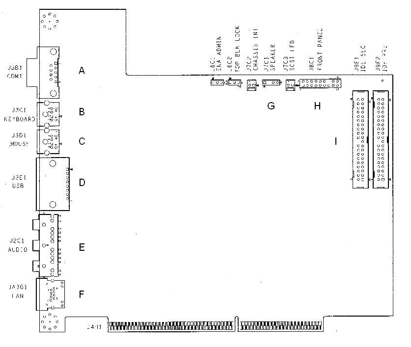
Figure 15. Baseboard Connectors
|
A. |
Serial Port Connector |
|
B. |
Keyboard Connector |
|
C. |
Mouse Connector |
|
D. |
USB Connector – NOT ACTIVE |
|
E. |
Audio Connector – NOT PRESENT |
|
F. |
LAN Connector – NOT PRESENT |
|
G. |
Speaker Connector |
|
H. |
Front Panel Connector |
|
I. |
IDE Connector |
Keyboard and Mouse Connectors
Figure 16. Keyboard and Mouse Connectors
The PS/2-compatible connectors share a common housing; they are not functionally equivalentinterchangeable.
|
Pin |
Keyboard signal |
Pin |
Mouse signal |
|
1 |
KEYDAT |
1 |
MSEDAT |
|
2 |
NC |
2 |
NC |
|
3 |
GND |
3 |
GND |
|
4 |
FUSED_VCC (+5 V) |
4 |
FUSED_VCC (+5 V) |
|
5 |
KEYCLK |
5 |
MSECLK |
|
6 |
NC |
6 |
NC |
Serial Port Connector
Figure 17. Serial Port Connector Pin out
|
Pin |
Signal |
Description |
|
1 |
DCD |
Data carrier detected |
|
2 |
RXD |
Receive data |
|
3 |
TXD |
Transmit data |
|
4 |
DTR |
Data terminal ready |
|
5 |
GND |
Ground |
|
6 |
DSR |
Data set ready |
|
7 |
RTS |
Request to send |
|
8 |
CTS |
Clear to send |
|
9 |
RIA |
Ring indication active |
|
PIN |
SIGNAL NAME |
|
1 |
LINK_LED |
|
2 |
Ground |
|
3 |
Unstuffed |
|
4 |
5VDC |
|
5 |
FP_RESET# |
|
6 |
Ground |
|
7 |
Unstuffed |
|
8 |
YEL_BLNK# |
|
9 |
Unstuffed |
|
10 |
GREEN/YELLOW_INV |
|
11 |
Unstuffed |
|
12 |
5VDC |
|
13 |
DASDACTIVE# |
|
14 |
Unstuffed |
|
15 |
5VDC |
|
16 |
Unstuffed |
|
17 |
IRSL1 |
|
18 |
IRTX |
|
19 |
Ground |
|
20 |
IRRX |
|
21 |
Unstuffed |
|
22 |
5VDC |
|
23 |
Unstuffed |
|
24 |
5VDC |
|
25 |
NC |
|
26 |
Ground |
|
27 |
PWR_SWITCH |
IDE Connectors
|
Pin |
Signal Name |
Pin |
Signal Name |
|
1 |
RST IDE |
2 |
GND |
|
3 |
Data 7 |
4 |
Data 8 |
|
5 |
Data 6 |
6 |
Data 9 |
|
7 |
Data 5 |
8 |
Data 10 |
|
9 |
Data 4 |
10 |
Data 11 |
|
11 |
Data 3 |
12 |
Data 12 |
|
13 |
Data 2 |
14 |
Data 13 |
|
15 |
Data 1 |
16 |
Data 14 |
|
17 |
Data 0 |
18 |
Data 15 |
|
19 |
GND |
20 |
KEY |
|
21 |
DMARQA [DMARQB] |
22 |
GND |
|
23 |
I/O Write # |
24 |
GND |
|
25 |
I/O Read # |
26 |
GND |
|
27 |
IORDY |
28 |
P_ALE [S_ALE](Cable Select Gnd) |
|
29 |
DMACKA# [DDACKB#] |
30 |
GND |
|
31 |
IRQ 14 [IRQ 15] |
32 |
RSVD |
|
33 |
PDA(1) |
34 |
RSVD |
|
35 |
PDA(0) |
36 |
PDA(2) |
|
37 |
Chip Select 1P# [Chip Select 1S#] |
38 |
Chip Select 3P# [Chip Select 3S#] |
|
39 |
LED # |
40 |
GND |
Note:
Signal names in brackets ([ ]) are for the secondary IDE connector|
Pin |
Signal Name |
|
1 |
HD_LED# |
|
2 |
Ground |
|
Pin |
Signal Name |
|
1 |
GND |
|
2 |
Audio Left Out |
|
3 |
Audio Right Out |
There are two- (2) chassis intrusion headers: One for the front of the chassis and one for the rear of the chassis.
|
Pin |
Signal Name |
|
1 |
TAMPER_DETECT# |
|
2 |
Ground |
USB Port
|
Pin |
Signal Name |
|
1 |
Power (fused) |
|
2 |
USBP0- [USBP1-] |
|
3 |
USBP0+[USBP1+] |
|
4 |
GND |
|
Pin |
Signal Name |
|
1 |
Power (fused) |
|
2 |
USBP0- [USBP1-] |
|
3 |
USBP0+[USBP1+] |
|
4 |
GND |
|
Pin |
Signal Name |
|
1 |
GND |
|
2 |
Audio Left In |
|
3 |
Audio Right In |
| . CACHE Enable (J6C1-IO Card) | |
|
CACHE on |
1-2* |
|
CACHE off |
2-3 |
|
*Default |
|
(This Page Left Intentionally Blank)
|
FSB FREQ MHz |
JUMPER SELECTION |
CLK GEN SELECTS |
||||||
|
J8C1 |
J9C1 |
J9C2 |
M<8..0> |
N<1..0> |
||||
|
66.666 |
1-2 |
4-5 |
2-3 |
4-5 |
1-2 |
100000000 |
0 |
1 |
|
75 |
2-3 |
4-5 |
2-3 |
4-5 |
1-2 |
100100000 |
0 |
1 |
|
100 |
1-2 |
4-5 |
2-3 |
4-5 |
2-3 |
110000000 |
0 |
1 |
|
125 |
2-3 |
5-6 |
2-3 |
4-5 |
2-3 |
111100000 |
0 |
1 |
|
133.333 |
1-2 |
4-5 |
1-2 |
4-5 |
1-2 |
100000000 |
0 |
0 |
|
150 |
2-3 |
4-5 |
1-2 |
4-5 |
1-2 |
100100000 |
0 |
0 |
|
166.667 |
1-2 |
5-6 |
1-2 |
4-5 |
1-2 |
101000000 |
0 |
0 |
|
0=Jumper Installed 1=No Jumper Installed Assuming 16.66MHz XTAL Speed. |
||||||||
| J9E1 - FSB Connector) | |
|
JTAG LOOP |
|
|
PROCESSOR LOOP |
1-2* |
|
SYSTEM |
2-3 |
|
*Default |
|
|
NORM |
1-2* |
|
OVRD/CLRCMOS |
2-3 |
|
RECOVERY |
NO JMPR |
|
*Default |
|
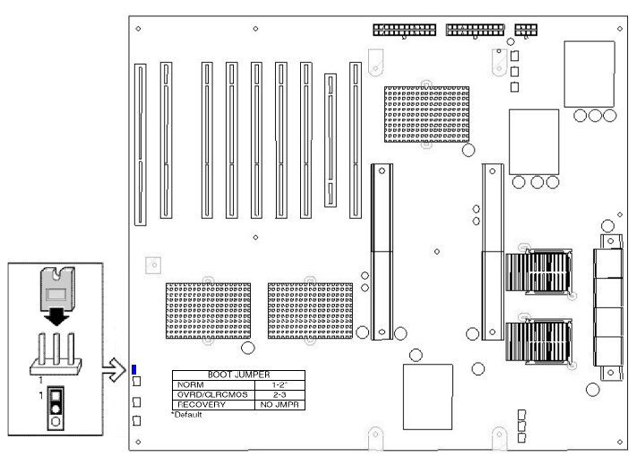
|
Table 37. JTAG MEMA (J5-G1-MEMA) |
|
|
BYPASS |
1-2* |
|
MEMA |
2-3 |
*Default |
|
|
Table 38. JTAG MEMB (J7-D1-MEMB) |
|
|
BYPASS |
1-2* |
|
MEMB |
2-3 |
|
*Default |
|